Pcb etching
Step-by-Step Guide to DIY PCB Etching
Printed Circuit Board (PCB) etching is a fundamental process in electronics manufacturing, allowing hobbyists and professionals alike to create custom circuit boards. This step-by-step guide to DIY PCB etching will walk you through the essential stages, ensuring a successful outcome.
To begin with, gather all necessary materials and tools.
You will need a blank copper-clad board, a laser printer, glossy paper, an iron, etching solution (ferric chloride or a similar etchant), a plastic container, protective gloves, safety goggles, and a drill for making holes. Once you have assembled these items, you can proceed to design your PCB layout using software such as Eagle, KiCad, or any other PCB design tool. After finalizing the design, print the layout onto glossy paper using a laser printer. The toner from the laser printer will act as a resist during the etching process.
Next, prepare the copper-clad board by cleaning it thoroughly with fine steel wool or a scouring pad to remove any oxidation and ensure a smooth surface.
This step is crucial as it allows the toner to adhere properly to the copper. After cleaning, rinse the board with water and dry it completely.
Following the preparation of the board, align the printed layout onto the copper surface, ensuring that the design is correctly positioned.
Using an iron set to its highest temperature, press the glossy paper onto the copper board. Apply firm, even pressure and move the iron in a circular motion for about 5-10 minutes. This process transfers the toner from the paper to the copper board. Once the board has cooled, carefully peel off the paper. The toner should now be adhered to the copper, forming a resist pattern that matches your design.
At this stage, inspect the board for any gaps or imperfections in the toner transfer.
If necessary, use a permanent marker to touch up any areas where the toner did not adhere properly. This step ensures that the etching solution will only remove the exposed copper, leaving the desired circuit pattern intact.
Now, prepare the etching solution by pouring it into a plastic container.
Always wear protective gloves and safety goggles when handling the etchant, as it is a corrosive substance. Submerge the copper board into the solution, agitating it gently to ensure even exposure. The etching process can take anywhere from 30 minutes to an hour, depending on the strength of the solution and the temperature. Monitor the progress closely, and once the unwanted copper has been dissolved, remove the board from the solution and rinse it thoroughly with water to stop the etching process.
After rinsing, remove the toner resist by scrubbing the board with acetone or a similar solvent.
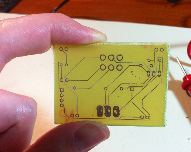
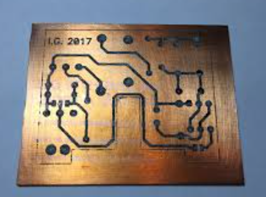
This will reveal the copper traces that form your circuit. Finally, drill any necessary holes for components using a small drill bit, and your PCB is ready for assembly.
In conclusion, DIY PCB etching is a meticulous yet rewarding process that allows for the creation of custom circuit boards. By following these steps carefully and taking appropriate safety precautions, you can achieve professional-quality results in your own workspace.
Top Chemicals Used in PCB Etching and Their Safety Measures
Printed Circuit Board (PCB) etching is a critical process in the manufacturing of electronic devices, involving the removal of unwanted copper from a copper-clad board to create the desired circuit pattern. This process relies heavily on specific chemicals, each with unique properties and safety considerations. Understanding the top chemicals used in PCB etching and their associated safety measures is essential for ensuring both effective etching and a safe working environment.
One of the most commonly used chemicals in PCB etching is ferric chloride (FeCl3).
Ferric chloride is favored for its effectiveness in dissolving copper, making it a popular choice among hobbyists and professionals alike. However, it is important to note that ferric chloride is highly corrosive and can cause severe skin and eye irritation upon contact. To mitigate these risks, it is crucial to wear appropriate personal protective equipment (PPE), including gloves, safety goggles, and protective clothing. Additionally, working in a well-ventilated area or using fume extraction systems can help minimize inhalation of any harmful vapors.
Another widely used etchant is ammonium persulfate ((NH4)2S2O8).
Ammonium persulfate offers a cleaner etching process compared to ferric chloride, as it produces fewer residues. Despite its advantages, ammonium persulfate is also a strong oxidizing agent and can pose significant health hazards if not handled properly. Direct contact with the skin or eyes can result in burns, while inhalation of its dust or fumes can cause respiratory issues. Therefore, it is imperative to use PPE, such as gloves, goggles, and masks, and to ensure adequate ventilation when working with this chemical.
Cupric chloride (CuCl2) is another etchant used in PCB manufacturing, particularly in industrial settings.
Cupric chloride is effective in etching copper and can be regenerated, making it a cost-effective option for large-scale operations. However, similar to other etchants, cupric chloride is corrosive and can cause skin and eye irritation. Proper handling procedures, including the use of PPE and working in a controlled environment, are essential to prevent accidents and exposure.
Hydrochloric acid (HCl) is often used in combination with hydrogen peroxide (H2O2) to create an etching solution known as the “muriatic acid and hydrogen peroxide” method.
This mixture is highly effective in etching copper but poses significant safety risks. Both hydrochloric acid and hydrogen peroxide are corrosive and can cause severe burns upon contact with the skin or eyes. Moreover, the reaction between these chemicals can produce chlorine gas, which is toxic and can cause respiratory distress. To ensure safety, it is vital to use PPE, work in a well-ventilated area, and handle the chemicals with extreme caution.
In addition to the aforementioned chemicals, sodium persulfate (Na2S2O8) is another etchant used in PCB manufacturing.
Sodium persulfate is known for its stability and effectiveness in etching fine details. However, it is also a strong oxidizer and can pose health risks if not handled properly. As with other etchants, the use of PPE and proper ventilation are essential to minimize exposure and prevent accidents.
In conclusion, PCB etching involves the use of various chemicals, each with specific properties and associated safety measures. Ferric chloride, ammonium persulfate, cupric chloride, hydrochloric acid, hydrogen peroxide, and sodium persulfate are among the top chemicals used in this process. Ensuring the safe handling of these chemicals through the use of appropriate PPE, adequate ventilation, and adherence to safety protocols is crucial for protecting both the individuals involved and the environment. By understanding the properties and risks of these chemicals, manufacturers can achieve effective PCB etching while maintaining a safe and compliant workplace.
Comparing Different PCB Etching Techniques: Pros and Cons
Printed Circuit Board (PCB) etching is a critical process in the manufacturing of electronic devices, as it involves the removal of unwanted copper from a copper-clad board to create the desired circuit pattern. Various techniques are employed in PCB etching, each with its own set of advantages and disadvantages. Understanding these methods is essential for selecting the most appropriate technique for a given application.
One of the most traditional methods of PCB etching is the ferric chloride etching process.
Ferric chloride is a chemical compound that reacts with copper to dissolve it, leaving behind the desired circuit pattern. This method is widely used due to its simplicity and cost-effectiveness. Ferric chloride is relatively inexpensive and readily available, making it an attractive option for hobbyists and small-scale manufacturers. However, this technique has several drawbacks. The etching process can be slow, and the chemical itself is highly corrosive and toxic, posing significant handling and disposal challenges. Additionally, ferric chloride can produce uneven etching, leading to potential defects in the circuit pattern.
Another commonly used technique is the ammonium persulfate etching process.
Ammonium persulfate is a strong oxidizing agent that effectively removes copper from the PCB. This method offers several advantages over ferric chloride etching. It produces a cleaner and more precise etch, which is crucial for high-density circuit designs. Furthermore, ammonium persulfate is less corrosive and easier to handle, reducing the risks associated with chemical exposure. However, the cost of ammonium persulfate is higher than that of ferric chloride, which can be a limiting factor for some users. Additionally, the disposal of ammonium persulfate requires careful consideration to avoid environmental contamination.
In contrast to chemical etching methods, the laser etching technique utilizes focused laser beams to remove copper from the PCB.
This method offers unparalleled precision and control, making it ideal for complex and high-resolution circuit designs. Laser etching is a non-contact process, which eliminates the risk of physical damage to the PCB. Moreover, it is a clean and environmentally friendly technique, as it does not involve the use of hazardous chemicals. However, the high cost of laser etching equipment and the need for specialized expertise can be significant barriers to its adoption. This technique is typically reserved for high-end applications where precision and quality are paramount.
Another advanced method is the plasma etching process, which uses ionized gas to remove copper from the PCB.
Plasma etching offers several benefits, including high precision, uniform etching, and the ability to etch through multiple layers of material. This technique is particularly useful for creating intricate and multi-layered circuit designs. Additionally, plasma etching is a dry process, eliminating the need for chemical handling and disposal. However, the complexity and cost of plasma etching equipment can be prohibitive for many users. This method is generally employed in specialized applications where its unique advantages outweigh the associated costs.
In conclusion, each PCB etching technique has its own set of pros and cons, making it essential to carefully consider the specific requirements of the application before selecting a method. Ferric chloride etching is cost-effective and accessible but poses handling and disposal challenges. Ammonium persulfate etching offers cleaner results but at a higher cost. Laser etching provides unmatched precision but requires significant investment in equipment and expertise. Plasma etching delivers high precision and uniformity but is also costly and complex. By weighing these factors, manufacturers can choose the most suitable etching technique to achieve the desired balance of performance, cost, and environmental impact.
Common Mistakes to Avoid During PCB Etching
PCB etching is a critical process in the manufacturing of printed circuit boards, where unwanted copper is removed to create the desired circuit patterns. However, this process is fraught with potential pitfalls that can compromise the quality and functionality of the final product.
One common mistake is the improper cleaning of the copper-clad board before etching.
Any residual grease, oil, or dirt can prevent the etchant from uniformly removing the copper, leading to incomplete or uneven etching. Therefore, it is essential to thoroughly clean the board using appropriate solvents and ensure it is completely dry before proceeding.
Another frequent error involves the incorrect application of the photoresist.
The photoresist layer must be uniformly applied to ensure that the etching process accurately follows the intended design. Inconsistent application can result in areas where the etchant either over-etches or under-etches, leading to circuit defects. To avoid this, it is advisable to use a high-quality photoresist and apply it in a controlled environment to minimize the risk of contamination.
Temperature control during the etching process is another critical factor that is often overlooked.
The etching solution must be maintained at an optimal temperature to ensure efficient and consistent etching. If the temperature is too low, the etching process will be slow and may not fully remove the unwanted copper. Conversely, if the temperature is too high, the etchant can become overly aggressive, leading to over-etching and potential damage to the circuit paths. Therefore, it is crucial to monitor and regulate the temperature of the etching solution carefully.
In addition to temperature, the concentration of the etching solution plays a significant role in the success of the etching process.
An incorrect concentration can lead to either an overly aggressive or insufficient etching action. It is important to follow the manufacturer’s guidelines for the preparation and maintenance of the etching solution to ensure optimal performance. Regularly checking and adjusting the concentration can help avoid issues related to under-etching or over-etching.
Furthermore, the duration of the etching process must be carefully controlled.
Leaving the board in the etching solution for too long can result in over-etching, where the etchant removes more copper than intended, potentially damaging the circuit paths. On the other hand, insufficient etching time can leave unwanted copper on the board, leading to short circuits or other functional issues. It is essential to monitor the etching process closely and remove the board from the solution at the appropriate time.
Another common mistake is the improper handling of the etched board.
After the etching process is complete, the board must be thoroughly rinsed to remove any residual etchant. Failure to do so can result in continued etching, which can damage the circuit paths. Additionally, the board should be handled with care to avoid scratching or damaging the delicate circuit patterns.
Lastly, inadequate inspection and testing of the etched board can lead to undetected defects that may cause issues during the assembly or operation of the final product.
It is important to conduct a thorough inspection of the etched board to identify and address any defects before proceeding to the next stage of manufacturing.
In conclusion, avoiding these common mistakes during the PCB etching process is crucial for producing high-quality printed circuit boards. By paying careful attention to cleaning, photoresist application, temperature control, etching solution concentration, etching duration, handling, and inspection, manufacturers can significantly improve the reliability and performance of their PCBs.


