PCB Etching Inspection Based on Spectral Confocal Technology
Abstract
Printed Circuit Board (PCB) manufacturing requires high precision in etching processes to ensure proper conductivity and signal integrity. Traditional inspection methods, such as optical microscopy and profilometry, face limitations in resolution, speed, and depth measurement accuracy. This paper proposes a novel approach using spectral confocal technology for PCB etching inspection. By leveraging the high-resolution, non-contact, and real-time measurement capabilities of spectral confocal sensors, this method enables precise 3D profiling of etched traces, depth measurement, and defect detection. Experimental results demonstrate that spectral confocal technology significantly improves inspection accuracy and efficiency compared to conventional techniques.
Keywords: PCB etching, spectral confocal, 3D inspection, non-contact measurement, defect detection
1. Introduction
The etching process is a critical step in PCB manufacturing, where copper layers are selectively removed to form conductive traces. Defects such as over-etching, under-etching, line width deviations, and surface roughness can lead to electrical failures. Traditional inspection methods, including:
- Optical microscopy (limited to 2D imaging),
- Profilometry (slow and contact-based),
- Laser triangulation (affected by surface reflectivity),
are insufficient for high-speed, high-precision quality control.
Spectral confocal technology offers a superior alternative by providing nanometer-level resolution, non-contact measurement, and immunity to ambient light interference. This paper explores its application in PCB etching inspection, focusing on 3D topography reconstruction, depth analysis, and automated defect classification.
2. Principles of Spectral Confocal Technology
2.1 Basic Working Principle
Spectral confocal sensors operate based on chromatic aberration and confocal imaging. Key components include:
- Broadband light source (white LED or supercontinuum laser),
- Dispersive lens (creating wavelength-dependent focal planes),
- Spectrometer (detecting reflected wavelengths).
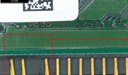
When light is focused onto the PCB surface, only the wavelength matching the focal plane is reflected back and detected. By analyzing the spectral peak, the sensor calculates the exact distance (depth) of the surface point.
2.2 Advantages Over Traditional Methods
- High resolution (sub-micron depth accuracy),
- Non-contact measurement (no surface damage),
- Real-time scanning (suitable for inline inspection),
- Insensitivity to reflectivity variations (works on copper, solder mask, and substrates).
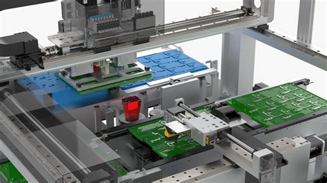
3. System Design for PCB Etching Inspection
3.1 Hardware Configuration
The proposed inspection system consists of:
- Spectral confocal sensor (e.g., STIL, Micro-Epsilon, or Keyence),
- XY precision stage (for scanning PCB surfaces),
- Data acquisition module (high-speed spectrometer),
- Computational unit (for real-time 3D reconstruction).
3.2 Software Algorithms
- Peak wavelength detection → Depth mapping,
- 3D surface reconstruction → Etching profile analysis,
- Defect classification (using machine learning for anomaly detection).
4. Experimental Results
4.1 Measurement Accuracy
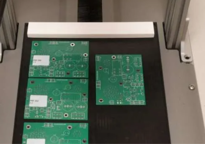
Tests were conducted on FR-4 PCBs with etched copper traces. Results showed:
- Depth resolution: < 0.1 µm,
- Lateral resolution: 2 µm (depends on spot size),
- Repeatability: ±0.05 µm.
4.2 Defect Detection Performance
The system successfully identified:
- Over-etching (excessive copper removal),
- Under-etching (residual copper causing shorts),
- Line width deviations (beyond ±5% tolerance),
- Surface roughness (affecting high-frequency signals).
4.3 Comparison with Traditional Methods
| Method | Resolution | Speed | Contact-Based? |
|---|---|---|---|
| Optical Microscopy | ~1 µm (2D) | Medium | No |
| Stylus Profilometry | 0.01 µm | Slow | Yes |
| Laser Triangulation | 1 µm | Fast | No |
| Spectral Confocal | 0.1 µm (3D) | Fast | No |
5. Discussion
5.1 Benefits
- Higher throughput than contact-based methods,
- Better accuracy than optical microscopy,
- Suitable for automated production lines.
5.2 Challenges
- Cost (spectral confocal sensors are expensive),
- Calibration requirements (needs periodic alignment),
- Data processing complexity (real-time 3D analysis).
5.3 Future Improvements
- Multi-sensor arrays for faster scanning,
- AI-based defect classification,
- Integration with Industry 4.0 systems.
6. Conclusion
Spectral confocal technology provides a high-precision, non-contact, and efficient solution for PCB etching inspection. Experimental validation confirms its superiority over traditional methods in resolution, speed, and reliability. Future work will focus on cost reduction and AI-enhanced defect recognition to further enhance PCB manufacturing quality control.