PCB Fabrication and Assembly: A Comprehensive Guide
Introduction
Printed circuit boards (PCBs) are the core components of modern electronic devices. Whether it is a mobile phone, computer or home appliance, almost all electronic products rely on PCBs to achieve electrical connections and signal transmission. The manufacturing and assembly process of PCBs is a complex and delicate project involving multiple steps and technologies. This article will explore the manufacturing and assembly process of PCBs in depth, including design, material selection, manufacturing process, assembly technology, and quality control.
1.PCB Design
PCB design is the first step in the entire manufacturing and assembly process. The design stage is usually carried out using electronic design automation (EDA) software, and designers need to consider the following aspects:
Circuit diagram design: First, designers need to create a circuit diagram to define the function and connection relationship of the circuit. The circuit diagram is the basis of PCB design, and all subsequent steps will be based on it.
Layout design: After the circuit diagram is completed, the designer needs to layout the circuit components on the PCB. This step needs to consider factors such as the distance between components, signal integrity, and heat dissipation. Reasonable layout can not only improve the performance of the PCB, but also reduce manufacturing costs.
Design Rule Check (DRC): After completing the layout, the designer needs to perform a design rule check to ensure that the design meets the manufacturer’s requirements. This includes checking parameters such as line width, spacing, aperture, etc.
Generate Gerber files: After the design is completed, the designer will generate Gerber files, which contain all the manufacturing information of the PCB and are the basis of PCB manufacturing.
2.PCB material selection
The performance of the PCB depends largely on the selected material. Common PCB materials include:
Substrate: FR-4 is the most commonly used PCB substrate, with good insulation properties and mechanical strength. For high-frequency applications, PTFE (polytetrafluoroethylene) material may be selected.
Copper foil: The conductive lines on the PCB are usually made of copper foil, and the thickness of copper is usually 1 ounce (about 35 microns) or thicker.
Solder mask: The solder mask is used to protect the lines on the PCB from short circuits and oxidation. Usually a green epoxy resin material is used.
Silk screen layer: The silk screen layer is used to identify component locations and other information, usually using white or black ink.
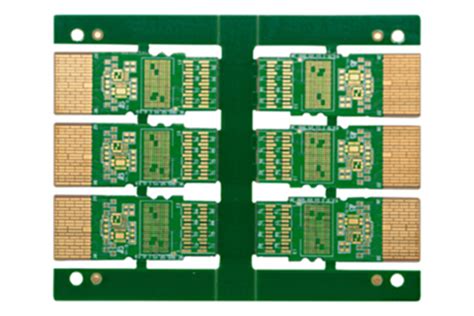
3.PCB Manufacturing Process
The manufacturing process of PCB usually includes the following steps:
(1)Material Preparation
First, the manufacturer will prepare the required substrate and copper foil. The substrate is usually a sheet made of glass fiber and resin.
(2)Copper Cladding
The copper foil is attached to the substrate to form a copper clad board. This process can be achieved by hot pressing or chemical copper plating.
(3)Photolithography
Photolithography is a key step in PCB manufacturing. The manufacturer will apply photosensitive material to the copper clad board and then use a light source to irradiate it to form a circuit pattern. The unexposed part will be removed by development, leaving the desired circuit pattern.
(4)Etching
After the photolithography is completed, the PCB will be etched to remove excess copper and finally form a circuit pattern. Etching usually uses chemicals such as ferric chloride or copper sulfate.
(5)Removal of photosensitive material
After etching, the manufacturer will remove the photosensitive material, leaving a clean copper line.
(6)Drilling
According to the design requirements, the manufacturer will drill holes in the PCB to install components and make electrical connections. Drilling can be done with a laser or a mechanical drill.
(7)Plating
For holes that need to be plated, the manufacturer will plate a layer of copper inside the hole to ensure the conductivity of the hole.
(8)Applying solder mask
After the electroplating is completed, the manufacturer will apply a solder mask on the PCB to protect the circuit and prevent short circuits during soldering.
(9)Silkscreen
Finally, the manufacturer will silkscreen on the PCB to identify the component location and other information.
(10)Cutting and testing
After manufacturing is completed, the PCB will be cut to the required size and electrically tested to ensure that it functions properly.
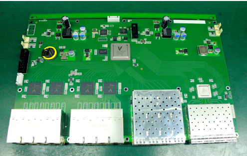
4. PCB Assembly
PCB assembly is the process of installing electronic components on the PCB. This process usually includes the following steps:
(1)Component preparation
Before assembly, the manufacturer needs to prepare all the electronic components, including resistors, capacitors, integrated circuits, etc. The components can be sorted and organized manually or automatically.
(2)Printing solder paste
On the soldering points of the PCB, the manufacturer will print solder paste. Solder paste is a sticky substance containing solder particles and flux, which is used to connect components and PCBs.
(3)Component placement
Using an automatic placement machine, electronic components are placed in the designated position of the PCB. This process requires high precision to ensure the correct position of the components.
(4)Reflow soldering
After the component placement is completed, the PCB will go through the reflow soldering process. The PCB is heated to a certain temperature to melt the solder paste and form a strong connection.
(5)Cleaning
After soldering is completed, the PCB will be cleaned to remove residual flux and impurities.
(6)Testing
Finally, the assembled PCB will undergo functional testing to ensure that all components are working properly. This includes electrical testing and functional testing.
5. Quality control
Quality control is crucial during the manufacturing and assembly process of PCBs. Manufacturers usually take the following measures to ensure product quality:
Raw material inspection: All raw materials are inspected to ensure that they meet the standards.
Process monitoring: During the manufacturing and assembly process, each link is monitored in real time to detect potential problems.
Final inspection: A comprehensive inspection of the finished product, including appearance inspection, electrical testing, and functional testing.
Reliability testing: Environmental testing and aging testing are performed to evaluate the performance of the PCB under different conditions.
Conclusion
The manufacturing and assembly of PCBs is a complex and delicate process involving multiple steps and technologies. With the continuous development of electronic technology, the design and manufacturing process of PCBs are also constantly improving. Understanding the manufacturing and assembly process of PCBs helps us better understand the working principles of electronic products, and also provides an important reference for practitioners in related industries. By continuously optimizing the design and manufacturing process, we can produce higher performance and more reliable PCBs to promote the sustainable development of the electronics industry.


