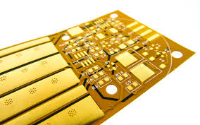
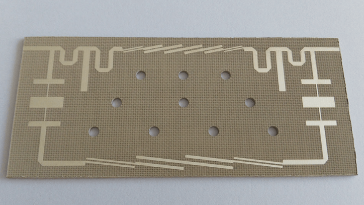
Pcb heavy copper
Advantages Of Using Heavy Copper In PCB Design
Heavy copper in printed circuit board (PCB) design offers a multitude of advantages that significantly enhance the performance, reliability, and durability of electronic devices.
One of the primary benefits of using heavy copper in PCBs is its ability to handle higher current loads.
Traditional PCBs, which typically use copper traces with a thickness of 1 oz/ft², can struggle to manage high current applications. In contrast, heavy copper PCBs, with copper thicknesses ranging from 3 oz/ft² to 20 oz/ft² or more, can efficiently conduct higher currents without overheating or suffering from excessive voltage drops. This capability is particularly crucial in power electronics, automotive, and industrial applications where robust current handling is essential.
Moreover, heavy copper PCBs exhibit superior thermal management properties.
The increased copper thickness allows for better heat dissipation, which is vital in preventing thermal buildup that can damage components and reduce the lifespan of the device. Effective thermal management ensures that the PCB operates within safe temperature ranges, thereby enhancing the overall reliability and performance of the electronic system. This is especially important in high-power applications where heat generation is a significant concern.
In addition to improved current handling and thermal management, heavy copper PCBs offer enhanced mechanical strength.
The thicker copper layers provide greater structural integrity, making the PCB more resistant to mechanical stresses such as bending, vibration, and thermal cycling. This increased durability is beneficial in harsh environments where electronic devices are subjected to rigorous conditions. For instance, in automotive and aerospace applications, where reliability and longevity are paramount, heavy copper PCBs can withstand the demanding operational environments better than their standard counterparts.
Another advantage of heavy copper PCBs is their ability to support complex and high-density designs.
The use of thicker copper allows for the creation of intricate circuit patterns and the integration of multiple layers without compromising the board’s performance. This capability is particularly advantageous in advanced electronic applications, such as telecommunications and medical devices, where compact and efficient designs are required. The flexibility in design also enables engineers to optimize the layout for better signal integrity and reduced electromagnetic interference (EMI), further enhancing the performance of the electronic system.
Furthermore, heavy copper PCBs contribute to cost savings in the long run.
Although the initial manufacturing cost of heavy copper PCBs may be higher than that of standard PCBs, their enhanced durability and reliability can lead to reduced maintenance and replacement costs over time. The ability to handle higher currents and better thermal management also means that fewer additional components, such as heat sinks and cooling systems, are needed, resulting in a more cost-effective overall design.
In conclusion, the use of heavy copper in PCB design offers numerous advantages that make it an attractive option for a wide range of applications. The ability to handle higher current loads, superior thermal management, enhanced mechanical strength, support for complex designs, and long-term cost savings are all compelling reasons to consider heavy copper PCBs. As electronic devices continue to evolve and demand higher performance and reliability, the adoption of heavy copper PCBs is likely to become increasingly prevalent in various industries.
Manufacturing Techniques For Heavy Copper PCBs
Heavy copper PCBs, characterized by their thick copper layers, are essential in applications requiring high current or enhanced thermal management. The manufacturing techniques for these robust circuit boards are more complex than those for standard PCBs, necessitating specialized processes to ensure reliability and performance. Understanding these techniques is crucial for engineers and manufacturers aiming to produce high-quality heavy copper PCBs.
The initial step in manufacturing heavy copper PCBs involves selecting the appropriate base material.
Typically, FR-4, a glass-reinforced epoxy laminate, is used due to its excellent mechanical and electrical properties. However, for heavy copper applications, the base material must be able to withstand higher temperatures and mechanical stresses. Therefore, materials with higher thermal conductivity and stability are often chosen to support the thick copper layers.
Once the base material is selected, the next phase is the application of the copper layers.
In standard PCBs, copper layers are usually 1 oz/ft² (35 µm) thick. In contrast, heavy copper PCBs have copper layers ranging from 3 oz/ft² (105 µm) to 20 oz/ft² (700 µm) or more. To achieve these thicknesses, a process called electroplating is employed. Electroplating involves immersing the PCB in a copper sulfate solution and applying an electric current, which deposits copper ions onto the board. This method allows for precise control over the thickness of the copper layers, ensuring uniformity and consistency.
Following the electroplating process, the next critical step is etching.
Etching removes unwanted copper to create the desired circuit patterns. For heavy copper PCBs, this process is more challenging due to the increased thickness of the copper layers. Traditional etching methods may not be sufficient, so advanced techniques such as differential etching are used. Differential etching involves using a combination of chemical and mechanical processes to achieve the necessary precision and accuracy.
After etching, the PCB undergoes a series of drilling and hole preparation steps.
Drilling is performed using high-speed CNC machines equipped with specialized drill bits capable of handling the thick copper layers. The holes are then plated with copper to ensure electrical connectivity between the different layers of the PCB. This step is particularly important for heavy copper PCBs, as the increased copper thickness can make it more difficult to achieve reliable interconnections.
Subsequently, the PCB is subjected to a series of inspections and tests to ensure its quality and performance.
These inspections include visual checks, electrical testing, and thermal cycling tests. Visual inspections help identify any defects or irregularities in the copper layers, while electrical testing ensures that the circuits function correctly. Thermal cycling tests are crucial for heavy copper PCBs, as they simulate the thermal stresses the board will experience in real-world applications, ensuring that it can withstand these conditions without failure.
Finally, the PCB is coated with a protective layer to prevent oxidation and improve its durability.
Common protective coatings include solder mask, which provides insulation and protection against environmental factors, and surface finishes such as HASL (Hot Air Solder Leveling) or ENIG (Electroless Nickel Immersion Gold), which enhance solderability and corrosion resistance.
In conclusion, the manufacturing techniques for heavy copper PCBs involve a series of specialized processes designed to handle the increased copper thickness and ensure the board’s reliability and performance. From selecting the appropriate base material to applying protective coatings, each step is critical in producing high-quality heavy copper PCBs capable of meeting the demanding requirements of high-current and thermal management applications.
Applications Of Heavy Copper PCBs In High-Power Electronics
Heavy copper PCBs, characterized by their thick copper layers, are increasingly becoming indispensable in the realm of high-power electronics. These specialized printed circuit boards are designed to handle higher currents and dissipate heat more effectively than standard PCBs, making them ideal for a variety of demanding applications. As the demand for more robust and reliable electronic devices continues to grow, the applications of heavy copper PCBs are expanding across multiple industries.
One of the primary applications of heavy copper PCBs is in power supply systems.
These systems require components that can manage high current loads without overheating or failing. Heavy copper PCBs are particularly well-suited for this purpose due to their enhanced thermal management capabilities. The thick copper layers allow for efficient heat dissipation, which is crucial in preventing thermal damage and ensuring the longevity of the components. Consequently, power supply manufacturers often rely on heavy copper PCBs to meet the stringent performance and reliability standards required in their products.
In addition to power supply systems, heavy copper PCBs are also extensively used in the automotive industry.
Modern vehicles are equipped with a multitude of electronic systems, ranging from engine control units to advanced driver-assistance systems (ADAS). These systems often operate under high current conditions and are subject to extreme temperatures. Heavy copper PCBs provide the necessary durability and thermal management to ensure these automotive electronics function reliably. Moreover, the ability of heavy copper PCBs to handle high currents makes them ideal for electric vehicles (EVs), where efficient power distribution is critical for optimal performance.
Another significant application of heavy copper PCBs is in industrial equipment.
Machinery and equipment used in industrial settings often require robust electronic components that can withstand harsh operating conditions. Heavy copper PCBs offer the mechanical strength and thermal resilience needed to endure such environments. For instance, in motor controllers and industrial power converters, the thick copper layers help manage the high currents and heat generated during operation, thereby enhancing the overall reliability and efficiency of the equipment.
Furthermore, heavy copper PCBs are gaining traction in the renewable energy sector.
Solar power inverters and wind turbine controllers are examples of applications where high current handling and efficient heat dissipation are paramount. Heavy copper PCBs enable these renewable energy systems to operate efficiently and reliably, even under fluctuating load conditions. This not only improves the performance of the renewable energy systems but also contributes to their longevity, making them more cost-effective in the long run.
In the realm of telecommunications, heavy copper PCBs are used in high-power amplifiers and base stations.
These components require stable and reliable performance to ensure uninterrupted communication. The enhanced current carrying capacity and thermal management provided by heavy copper PCBs are essential in maintaining the performance and reliability of these critical communication systems.
In conclusion, the applications of heavy copper PCBs in high-power electronics are vast and varied. From power supply systems and automotive electronics to industrial equipment and renewable energy systems, heavy copper PCBs play a crucial role in ensuring the reliability and efficiency of high-power electronic devices. As technology continues to advance and the demand for more robust electronic components grows, the importance of heavy copper PCBs in high-power electronics is likely to increase, further solidifying their position as a key component in modern electronic design.
Cost Considerations And Benefits Of Heavy Copper PCBs
When evaluating the cost considerations and benefits of heavy copper PCBs, it is essential to understand the unique attributes that distinguish them from standard PCBs. Heavy copper PCBs, characterized by their thicker copper layers, typically ranging from 3 oz/ft² to 20 oz/ft², offer a range of advantages that justify their higher initial costs. These benefits are particularly relevant in applications requiring enhanced durability, superior thermal management, and increased current-carrying capacity.
One of the primary cost considerations associated with heavy copper PCBs is the increased material expense.
The thicker copper layers necessitate more raw material, which directly impacts the overall cost of production. Additionally, the manufacturing process for heavy copper PCBs is more complex and time-consuming compared to standard PCBs. Specialized techniques such as differential etching and step plating are often required to achieve the desired copper thickness, further contributing to the higher production costs. However, these initial expenses can be offset by the long-term benefits and reliability that heavy copper PCBs provide.
The enhanced durability of heavy copper PCBs is a significant benefit that can lead to cost savings over time.
These PCBs are designed to withstand harsh operating conditions, including high temperatures and mechanical stress. The robust construction reduces the likelihood of failure, thereby minimizing the need for frequent repairs or replacements. This reliability is particularly valuable in industries such as aerospace, automotive, and industrial equipment, where downtime can be costly and disruptive.
In addition to durability, heavy copper PCBs offer superior thermal management capabilities.
The thicker copper layers facilitate efficient heat dissipation, which is crucial for high-power applications. Effective thermal management helps prevent overheating and ensures the stable operation of electronic components. This can extend the lifespan of the PCB and the overall system, reducing maintenance costs and enhancing performance. Consequently, the investment in heavy copper PCBs can be justified by the improved thermal performance and the associated cost savings.
Another notable benefit of heavy copper PCBs is their increased current-carrying capacity.
The thicker copper layers allow for higher current flow without the risk of overheating or damage. This is particularly advantageous in power electronics, where high current levels are common. The ability to handle higher currents can lead to more efficient and compact designs, as fewer layers or additional components are needed to achieve the desired performance. This can result in cost savings in terms of both materials and assembly.
Furthermore, heavy copper PCBs can contribute to overall system cost reduction by enabling more efficient and reliable designs.
The enhanced electrical performance and thermal management capabilities can lead to simplified circuit layouts and reduced component count. This not only lowers the material costs but also streamlines the assembly process, reducing labor expenses and potential points of failure. The long-term reliability and performance of heavy copper PCBs can also enhance the reputation of the end product, potentially leading to increased customer satisfaction and repeat business.
In conclusion, while the initial costs of heavy copper PCBs are higher due to increased material requirements and complex manufacturing processes, the long-term benefits they offer can outweigh these expenses. The enhanced durability, superior thermal management, and increased current-carrying capacity make heavy copper PCBs a valuable investment for applications demanding high performance and reliability. By considering both the upfront costs and the long-term advantages, businesses can make informed decisions about incorporating heavy copper PCBs into their designs, ultimately leading to cost savings and improved product performance.


