PCB Interconnect Solutions: A Comprehensive Guide
Introduction to PCB Interconnection
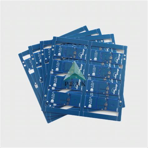
Printed Circuit Board (PCB) interconnections form the backbone of modern electronics, enabling the complex networks that power everything from smartphones to industrial machinery. As electronic devices become more sophisticated and compact, the challenges of creating reliable, high-performance interconnections between PCB components and boards have grown exponentially.
PCB interconnections serve three primary functions: power distribution to provide stable voltage levels across the board, signal transmission for data and control signals between components, and mechanical support to physically secure components in place. The quality of these interconnections directly impacts the overall performance, reliability, and longevity of electronic devices.
Current market trends show increasing demand for higher interconnection densities to support miniaturization, with the global PCB market projected to reach $89.7 billion by 2027. Emerging technologies like 5G, IoT, and AI are driving the need for more advanced interconnection solutions that can handle higher frequencies, greater power demands, and more complex signal integrity requirements.
Traditional PCB Interconnect Methods
Through-Hole Technology (THT)
Through-hole technology represents one of the earliest and most reliable PCB interconnection methods. In this approach, component leads are inserted through drilled holes in the PCB and soldered to pads on the opposite side. THT offers several advantages:
- Mechanical Strength: The through-hole construction provides excellent mechanical stability, making it ideal for components subject to physical stress.
- Reliability: The robust connections are less prone to failure from thermal cycling or vibration.
- Ease of Prototyping: THT is often preferred for prototyping and manual assembly processes.
However, THT has significant limitations in modern electronics:
- It consumes board space on both sides, limiting component density
- The drilling process adds manufacturing complexity and cost
- It’s unsuitable for very high-frequency applications due to longer lead lengths
Surface Mount Technology (SMT)
Surface mount technology revolutionized PCB design by allowing components to be mounted directly onto the surface of the board. SMT offers numerous advantages:
- Space Efficiency: Components can be placed on both sides of the board with much higher density
- Performance Benefits: Shorter leads reduce parasitic inductance and capacitance, enabling better high-frequency performance
- Manufacturing Advantages: SMT enables automated assembly processes, reducing production costs
Despite these benefits, SMT presents certain challenges:
- Smaller components can be more difficult to prototype and repair
- Solder joints may be more susceptible to thermal and mechanical stress
- Requires precise control of solder paste application and reflow processes
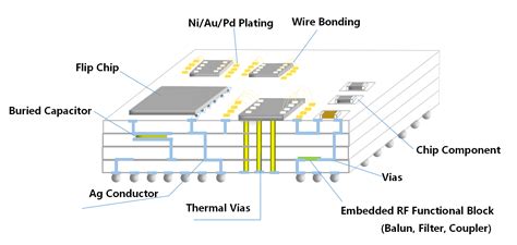
Wire Bonding
Wire bonding remains a crucial interconnection technique, particularly in semiconductor packaging. This method uses thin wires (typically gold, aluminum, or copper) to create connections between chips and their packages or substrates. Wire bonding offers:
- Flexibility: Can accommodate different chip and package configurations
- Cost-Effectiveness: Relatively low-cost equipment compared to some alternatives
- Maturity: Well-established process with decades of refinement
Limitations include:
- Speed constraints in high-volume production
- Potential for wire sweep or deformation in some applications
- Limited suitability for very high-frequency applications
Advanced PCB Interconnect Solutions
High-Density Interconnect (HDI) Technology
HDI technology has emerged as a solution for increasingly complex interconnection requirements. HDI PCBs feature:
- Microvias: Small laser-drilled vias (typically <150μm) that enable higher routing density
- Finer Traces and Spaces: Allows more connections in less space
- Sequential Lamination: Multiple lamination cycles to build complex interconnect structures
HDI offers significant advantages:
- Enables miniaturization of electronic devices
- Improves signal integrity by reducing path lengths
- Supports high pin-count packages like BGAs
Design considerations for HDI include:
- Careful via type selection (blind, buried, staggered, etc.)
- Material selection for optimal high-frequency performance
- Thermal management in dense layouts
Embedded Components
Embedded component technology takes interconnection to the next level by placing passive components (and sometimes actives) within the PCB layers. This approach offers:
- Space Savings: Frees up surface area for other components
- Performance Benefits: Shorter interconnects improve electrical performance
- Improved Reliability: Protected from environmental factors
Implementation challenges include:
- More complex design and manufacturing processes
- Limited reparability of embedded components
- Thermal management considerations
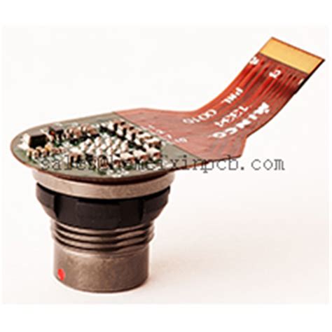
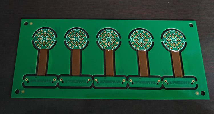
Flexible and Rigid-Flex Interconnects
Flexible PCB technologies provide unique interconnection solutions for modern electronics:
- Flex Circuits: Thin, lightweight interconnects that can bend and fold
- Rigid-Flex: Hybrid designs combining rigid and flexible sections
- 3D Configuration: Ability to fit into unconventional spaces
Applications span:
- Wearable electronics
- Medical devices
- Aerospace systems
- Consumer electronics with moving parts
Design considerations include:
- Bend radius requirements
- Material selection for flexibility and durability
- Connection points between rigid and flexible sections
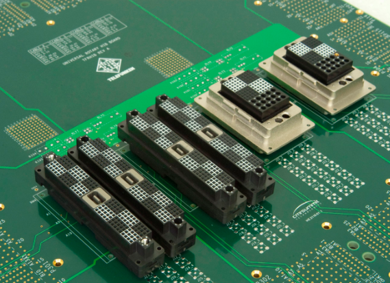
High-Speed and RF Interconnect Solutions
Transmission Line Structures
High-speed designs require careful consideration of transmission line effects. Common structures include:
- Microstrip: Conductor on outer layer with reference plane beneath
- Stripline: Conductor embedded between two reference planes
- Coplanar Waveguide: Conductor with adjacent ground planes on same layer
Design requirements for high-speed interconnects:
- Controlled impedance matching
- Careful attention to dielectric materials
- Minimization of discontinuities and reflections
RF and Microwave Interconnects
RF applications present unique interconnection challenges:
- Specialized Connectors: SMP, SMA, and other RF connectors
- Transition Structures: Smooth transitions between different transmission media
- Shielding Considerations: Preventing interference and signal leakage
Materials play a critical role in RF interconnects:
- Low-loss dielectric materials
- Surface finishes that maintain conductivity at high frequencies
- Consistent material properties across production runs
Signal Integrity Considerations
Maintaining signal integrity requires attention to:
- Crosstalk Mitigation: Proper spacing, guard traces, and ground shielding
- Impedance Control: Consistent characteristic impedance throughout the signal path
- Return Path Management: Ensuring uninterrupted reference planes
Simulation and analysis tools are essential for:
- Predicting signal behavior
- Identifying potential problem areas
- Optimizing interconnect designs
Emerging Interconnect Technologies
Photonic Interconnects
Photonic interconnects represent a promising future direction:
- Optical Waveguides: Embedded in PCBs for light transmission
- Hybrid Electrical/Optical Boards: Combining both technologies
- Benefits: Extremely high bandwidth, immunity to EMI, lower power for long-distance on-board communication
Current challenges include:
- Coupling between optical and electronic components
- Manufacturing complexity
- Cost considerations
3D and Heterogeneous Integration
Advanced packaging technologies are pushing interconnect boundaries:
- Through-Silicon Vias (TSVs): Vertical connections through silicon dies
- Package-on-Package (PoP): Stacking packaged components
- Chiplet Architectures: Interconnecting multiple dies in a package
These approaches enable:
- Continued performance scaling
- Improved form factors
- Heterogeneous integration of different technologies
Advanced Materials for Interconnects
New materials are enabling better interconnection performance:
- Low-Loss Laminates: For high-frequency applications
- Conductive Inks and Pastes: For printed electronics
- Nanomaterials: Such as carbon nanotubes and graphene for future interconnects
Selection Criteria for PCB Interconnect Solutions
Choosing the right interconnect solution requires considering multiple factors:
Technical Requirements
- Electrical Performance: Signal speed, power requirements, noise sensitivity
- Mechanical Requirements: Vibration, flexing, shock resistance
- Environmental Factors: Temperature, humidity, chemical exposure
Manufacturing Considerations
- Production Volume: High-volume vs. low-volume considerations
- Assembly Processes: Available equipment and expertise
- Testability: Access for testing and inspection
Cost Analysis
- Initial Development Costs: NRE for new technologies
- Production Costs: Material, labor, yield considerations
- Lifecycle Costs: Reliability, maintenance, repair
Future Trends in PCB Interconnection
The PCB interconnect landscape continues to evolve:
- Increased Adoption of HDI: As costs decrease and demand grows
- Growth of Flexible Electronics: For wearable and IoT applications
- Integration of More Functions: Combining power, data, and even fluidics in interconnects
- Sustainable Solutions: Environmentally friendly materials and processes
Industry 4.0 and IoT applications will drive:
- More robust interconnect solutions for harsh environments
- Higher reliability requirements
- Integration with sensors and smart functionalities

Conclusion
PCB interconnect solutions form a critical and rapidly evolving aspect of electronic design and manufacturing. From traditional through-hole technology to cutting-edge photonic interconnects and 3D integration, the field offers numerous options to meet diverse application requirements.
The key to successful PCB interconnection lies in understanding the trade-offs between performance, reliability, density, and cost. As electronic systems continue to advance, interconnection technologies must keep pace, enabling smaller, faster, and more complex devices while maintaining or improving reliability.
Designers and engineers must stay informed about emerging interconnect solutions while mastering established technologies. The future of PCB interconnections promises exciting developments that will continue to push the boundaries of what’s possible in electronic systems.