PCB Layout Guidelines for Photovoltaic Power Systems
Introduction
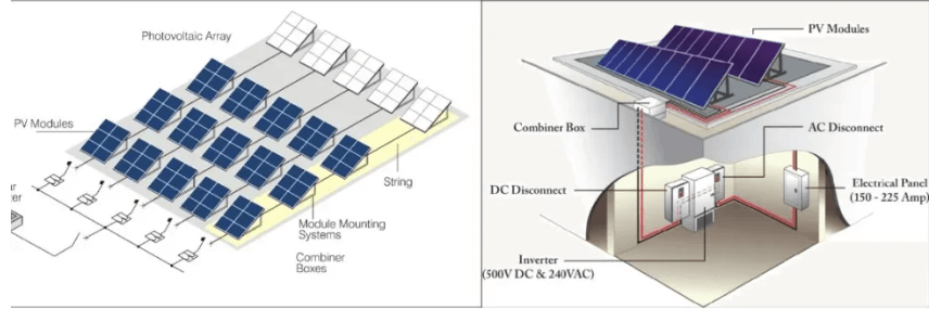
Photovoltaic (PV) power systems convert solar energy into electrical energy, and their performance heavily depends on the design of the printed circuit board (PCB). A well-optimized PCB layout ensures efficient power conversion, minimal losses, and reliable operation under varying environmental conditions. This article discusses key considerations for PCB layout in PV applications, including component placement, routing strategies, thermal management, and noise reduction techniques.
1. Component Placement
1.1 Power Stage Components
The power stage in a PV system typically includes:
- DC-DC Converters (Boost, Buck, or Buck-Boost)
- Maximum Power Point Tracking (MPPT) Controllers
- Inverters (for AC-coupled systems)
Key Guidelines:
- Place high-current components (MOSFETs, diodes, inductors) close to each other to minimize parasitic inductance.
- Position input capacitors near the PV panel terminals to reduce high-frequency noise.
- Keep feedback and control circuitry away from high-power traces to avoid interference.
1.2 Signal and Control Components
- Place analog sensing circuits (voltage/current sensors) near the measurement points.
- Keep digital control circuits (microcontrollers, gate drivers) separate from high-power sections.
- Use star grounding for sensitive analog components to prevent ground loops.
2. Routing Considerations
2.1 High-Current Traces
- Use wide traces (≥ 50 mils for 5A+) to minimize resistance and heat buildup.
- Avoid sharp angles; use 45° bends or curved traces to reduce impedance discontinuities.
- Implement copper pours for high-current paths to improve thermal dissipation.
2.2 High-Frequency Switching Nodes
- Keep switching node traces (e.g., MOSFET-to-inductor) as short as possible to reduce EMI.
- Use ground planes beneath high-frequency traces to provide a return path and reduce radiation.
2.3 Sensitive Signal Routing
- Route analog feedback signals (voltage, current sensing) away from noisy power traces.
- Use differential pairs for critical signals to improve noise immunity.
- Implement guard rings around sensitive traces to minimize capacitive coupling.
3. Thermal Management
3.1 Heat Dissipation Techniques
- Use large copper areas or thermal vias under power components (MOSFETs, diodes).
- Consider external heatsinks for high-power applications.
- Ensure proper airflow by avoiding component crowding.
3.2 Temperature Monitoring
- Place temperature sensors near hotspots (e.g., power inductors, switching FETs).
- Use thermal relief pads for components requiring soldering to prevent heat sinking during assembly.
4. Grounding and Noise Reduction
4.1 Ground Plane Strategy
- Use separate ground planes for analog and digital sections, connected at a single point.
- Avoid splitting ground planes under high-frequency switching circuits.
- Ensure low-impedance return paths for high-current loops.
4.2 EMI/EMC Mitigation
- Add snubber circuits (RC networks) across switching devices to dampen ringing.
- Use ferrite beads or common-mode chokes on input/output lines to suppress high-frequency noise.
- Implement shielding cans over sensitive RF sections if necessary.
5. PV-Specific Considerations
5.1 Handling Variable Input Voltage
- Ensure PCB traces and components can withstand open-circuit PV voltage (often 50V+ for small systems, 600V+ for grid-tied systems).
- Use proper creepage and clearance distances to prevent arcing.
5.2 Protection Circuits
- Place overvoltage protection (TVS diodes, varistors) near PV input terminals.
- Implement reverse-polarity protection (e.g., MOSFET-based or diode solutions).
- Ensure proper fuse placement to protect against short circuits.
6. Testing and Validation
6.1 Prototype Testing
- Verify efficiency at different irradiance levels (MPPT performance).
- Check thermal performance under maximum load.
- Conduct conducted/radiated EMI tests to ensure compliance.
6.2 Environmental Robustness
- Use conformal coating if the PCB is exposed to humidity or dust.
- Select components rated for extended temperature ranges (-40°C to +85°C for outdoor applications).
Conclusion
Designing a PCB for photovoltaic power systems requires careful attention to component placement, routing, thermal management, and noise control. By following these guidelines, engineers can optimize efficiency, reliability, and longevity of PV-based power electronics. Future advancements in wide-bandgap semiconductors (SiC/GaN) may further influence PCB layout strategies, enabling higher switching frequencies and power densities.