PCB layout techniques for optimizing power module performance
The global energy shortage problem has led governments around the world to vigorously promote new energy-saving policies. The energy consumption standards for electronic products are becoming increasingly stringent.
For power design engineers, how to design more efficient and high-performance power supplies is an eternal challenge. Starting from the layout of the power supply PCB, this article introduces the best PCB layout methods, examples and techniques for optimizing the performance of SIMPLE SWITCHER power modules.
When planning the power supply layout, the first thing to consider is the physical loop area of the two switching current loops.
Although these loop areas are basically invisible in the power module, it is still important to understand the current paths of each of the two loops because they extend outside the module. In loop 1 shown in Figure 1, the current self-conducts through the input bypass capacitor (Cin1) during the continuous conduction time of the high-side MOSFET through the MOSFET to the internal inductor and output bypass capacitor (CO1), and finally returns to the input bypass capacitor.
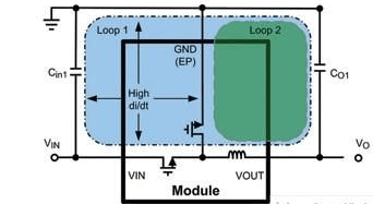
Figure 1 Schematic diagram of loops in power modules
Loop 2 is formed during the off time of the internal high-side MOSFET and the on time of the low-side MOSFET. The energy stored in the internal inductor flows through the output bypass capacitor and the low-side MOSFET and returns to GND (as shown in Figure 1). The area where the two loops do not overlap (including the boundary between the loops) is the high di/dt current region. The input bypass capacitor (Cin1) plays a key role in providing high-frequency current to the converter and returning it to its source path.
The output bypass capacitor (Co1) does not carry large AC currents, but it acts as a high-frequency filter for switching noise. For these reasons, the input and output capacitors should be placed as close to their respective VIN and VOUT pins as possible on the module. As shown in Figure 2, the inductance generated by these connections can be minimized by keeping the traces between the bypass capacitors and their respective VIN and VOUT pins as short and wide as possible.

Figure 2 SIMPLE SWITCHER Loop
Minimizing the inductance in the PCB layout has two major benefits. First, it improves component performance by facilitating the transfer of energy between Cin1 and CO1. This will ensure that the module has good high-frequency bypassing and minimize the inductive voltage peaks generated by high di/dt currents. At the same time, it can also minimize device noise and voltage stress to ensure its normal operation. Second, minimize EMI.
Connecting capacitors with less parasitic inductance will show low impedance characteristics to high frequencies, thereby reducing conducted radiation. Ceramic capacitors (X7R or X5R) or other low ESR capacitors are recommended. Adding more input capacitance can only work if the additional capacitance is placed close to the GND and VIN terminals. SIMPLE SWITCHER power modules are uniquely designed to have low radiated and conducted EMI, and following the PCB layout guidelines introduced in this article will achieve higher performance.
The path planning of the loop current is often overlooked, but it plays a key role in optimizing power supply design. In addition, the ground traces between Cin1 and CO1 should be shortened and widened as much as possible, and directly connected to the exposed pad, which is especially important for the ground connection of the input capacitor (Cin1) with large AC current.
The ground pins (including the exposed pad), input and output capacitors, soft start capacitors, and feedback resistors in the module should all be connected to the loop layer on the PCB. This loop layer serves as a very low return path for the inductor current and as a heat sink as discussed below.
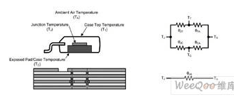
Figure 3 Schematic of the module and PCB as thermal impedance
The feedback resistor should also be placed as close to the module FB (feedback) pin as possible. It is critical to keep the trace between the FB pin and the center tap of the feedback resistor as short as possible to minimize potential noise pickup at this high impedance node. Available compensation components or feedforward capacitors should be placed as close to the upper feedback resistor as possible. For examples, refer to the PCB layout diagram given in the relevant module datasheet.
Thermal Design Recommendations
While the compact layout of the module brings electrical benefits, it has a negative impact on thermal design, as the same amount of power must be dissipated from a smaller space. With this in mind, the SIMPLE SWITCHER power module package is designed with a single large exposed pad on the back side and is electrically grounded. This pad helps provide very low thermal impedance from the internal MOSFET (which typically generates most of the heat) to the PCB.
The thermal impedance (θJC) from the semiconductor junction to the external package of these devices is 1.9℃/W. While achieving industry-leading θJC values is desirable, low θJC values are meaningless when the thermal impedance from package to air (θCA) is too great! If a low impedance heatsink path to the surrounding air is not provided, the heat will be trapped at the exposed pad and unable to dissipate. So what determines the θCA value? The thermal resistance from the exposed pad to air is completely controlled by the PCB design and the associated heat sink.
Now for a quick look at a simple PCB thermal design without a heat sink, Figure 3 shows the module and the PCB as the thermal impedance. When first estimating the thermal resistance from junction to ambient air (θJT), we can ignore the θJA thermal path because the thermal impedance from junction to top of package is relatively high compared to the thermal impedance from junction to die pad.
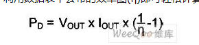
The first step in thermal design is to determine the power to be dissipated. The power dissipated by the module (PD) can be easily calculated using the efficiency graph (η) published in the datasheet.
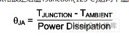
We then use the two temperature constraints of the maximum temperature in the design, TAmbient, and the rated junction temperature, TJunction (125°C), to determine the required thermal resistance of the module packaged on the PCB.
Finally, we use the maximum simplified approximation of convective heat transfer on the PCB surface (with an undamaged one-ounce copper heat sink and numerous vias on both the top and bottom layers) to determine the board area required for heat dissipation.
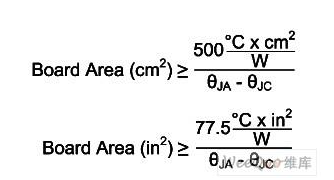
The required PCB board area approximation does not take into account the role played by the vias, which transfer heat from the top metal layer (where the package connects to the PCB) to the bottom metal layer. The bottom layer acts as a second surface layer from which convection can transfer heat away from the board. For the board area approximation to be valid, at least 8 to 10 vias are used. The thermal resistance of the vias is approximated by the following equation.
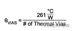
This approximation is for a typical straight-through via with a diameter of 12 mils and a copper sidewall of 0.5 ounces. Design as many vias as possible throughout the area under the exposed pad and form an array with 1 to 1.5 mm spacing.
Conclusion
The SIMPLE SWITCHER power modules provide an alternative to the complex power supply designs and typical PCB layouts associated with DC/DC converters. While the layout challenges are eliminated, some engineering work still needs to be done to optimize module performance with good bypassing and thermal design.