PCB Manufacturing and Assembly: A Comprehensive Overview
Introduction
Printed Circuit Boards (PCBs) are essential components in modern electronic devices, serving as the backbone that connects and supports electronic components. The manufacturing and assembly of PCBs involve intricate processes that ensure the reliability and functionality of electronic products. This article provides a comprehensive overview of PCB manufacturing and assembly, discussing the various stages, technologies, and best practices involved in creating high-quality PCBs.
1. Understanding PCBs
1.1 Definition and Function
A Printed Circuit Board is a flat board made of insulating material, typically fiberglass, with conductive pathways etched onto its surface. These pathways, made of copper, connect various electronic components such as resistors, capacitors, and integrated circuits. PCBs can be single-sided, double-sided, or multi-layered, depending on the complexity of the circuit design.
1.2 Types of PCBs
- Single-Sided PCBs: These have components mounted on one side and are used for simple circuits.
- Double-Sided PCBs: These feature components on both sides, allowing for more complex designs.
- Multi-layer PCBs: These consist of multiple layers of conductive pathways, enabling high-density circuits found in advanced electronics.
- Flexible PCBs: Made from flexible materials, these PCBs can bend and twist, making them suitable for compact and portable devices.
- Rigid-Flex PCBs: A combination of rigid and flexible circuit boards, used in applications where space and weight are critical.
2. PCB Manufacturing Process
The manufacturing process of PCBs involves several key steps, each critical to ensuring the final product meets quality standards.
2.1 Design and Layout
The first step in PCB manufacturing is the design phase, where engineers use Computer-Aided Design (CAD) software to create the circuit layout. This design includes the placement of components, routing of electrical connections, and specifications for the PCB’s dimensions and layers. Important considerations during this phase include signal integrity, thermal management, and manufacturability.
2.2 Printing the PCB
Once the design is finalized, the next step is to print the PCB. This involves several sub-steps:
- Film Generation: The design is printed onto a film, which serves as a mask for the subsequent processes.
- Substrate Preparation: The PCB substrate, typically made of FR-4 (a fiberglass epoxy), is cleaned and prepared for coating.
- Copper Foil Lamination: A layer of copper foil is laminated onto the substrate, providing the conductive pathways.
2.3 Etching
The etching process removes excess copper from the board, leaving behind the desired circuit pattern. This is typically done using chemical etchants that dissolve the unwanted copper. The board is then cleaned to remove any residual chemicals.
2.4 Drilling
After etching, holes are drilled into the PCB for component leads and vias (vertical connections between layers). This step requires precision, as the hole sizes must match the component specifications.
2.5 Plating
The drilled holes are plated with copper to create conductive pathways between layers. This process often involves electroplating, where a thin layer of copper is deposited onto the walls of the drilled holes.
2.6 Solder Mask Application
A solder mask is applied to the PCB to protect the copper traces from oxidation and to prevent solder bridges during assembly. This layer is typically green, but other colors are available.
2.7 Surface Finish
To ensure good solderability, a surface finish is applied to the exposed copper pads. Common finishes include HASL (Hot Air Solder Leveling), ENIG (Electroless Nickel Immersion Gold), and OSP (Organic Solderability Preservative).
2.8 Testing
Before moving on to assembly, the PCBs undergo testing to identify any defects. This can include electrical testing, visual inspections, and automated optical inspection (AOI).
3. PCB Assembly Process
Once the PCBs are manufactured, they are ready for assembly, where electronic components are mounted onto the boards.
3.1 Component Placement
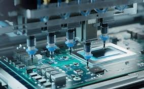
The first step in assembly is the placement of components onto the PCB. This can be done manually or using automated pick-and-place machines, which accurately position components based on the design files.
3.2 Soldering
After placement, components are soldered to the PCB. There are several soldering methods:
- Wave Soldering: Used primarily for through-hole components, where the PCB is passed over a wave of molten solder.
- Reflow Soldering: Common for surface-mount devices (SMDs), where solder paste is applied to the pads, and the board is heated in a reflow oven to melt the solder.
- Hand Soldering: Used for repairs or low-volume production, where a soldering iron is used to manually solder components.
3.3 Inspection and Testing
Following soldering, the assembled PCBs undergo inspection and testing to ensure quality and functionality. This may include visual inspections, X-ray inspection for hidden solder joints, and functional testing to verify that the circuit operates as intended.
3.4 Final Assembly
Once the PCBs pass inspection, they may undergo final assembly, where they are integrated into larger systems or enclosures. This step may involve additional components, such as connectors, displays, and housings.
4. Quality Control in PCB Manufacturing and Assembly
Quality control is crucial throughout the PCB manufacturing and assembly process. Implementing rigorous quality assurance practices helps identify defects early and ensures that the final product meets industry standards.
4.1 Standards and Certifications
Several industry standards govern PCB manufacturing and assembly, including IPC-A-600 (Acceptability of Printed Boards) and IPC-A-610 (Acceptability of Electronic Assemblies). Obtaining certifications such as ISO 9001 can also enhance credibility and demonstrate a commitment to quality.
4.2 Process Control
Monitoring key process parameters, such as temperature, humidity, and chemical concentrations, is essential for maintaining consistent quality. Statistical Process Control (SPC) techniques can be employed to analyze data and identify trends that may indicate potential issues.
4.3 Continuous Improvement
Adopting a culture of continuous improvement allows manufacturers to refine processes, reduce waste, and enhance product quality. Techniques such as Six Sigma and Lean Manufacturing can be beneficial in achieving these goals.
5. Future Trends in PCB Manufacturing and Assembly
As technology advances, the PCB manufacturing and assembly industry continues to evolve. Some notable trends include:
5.1 Miniaturization
The demand for smaller and more compact electronic devices drives the need for miniaturized PCBs. Innovations in materials and manufacturing techniques are enabling the production of smaller, high-density circuits.
5.2 Advanced Materials
New materials, such as high-frequency substrates and flexible materials, are being developed to meet the requirements of emerging technologies like 5G and Internet of Things (IoT) devices.
5.3 Automation and Industry 4.0
The integration of automation and smart technologies into PCB manufacturing and assembly processes is enhancing efficiency and reducing human error. Industry 4.0 concepts, such as the Internet of Things and data analytics, are being adopted to optimize production and supply chain management.
5.4 Environmental Sustainability
As environmental concerns grow, the PCB industry is focusing on sustainable practices, such as reducing waste, recycling materials, and using eco-friendly chemicals in the manufacturing process.
Conclusion
The manufacturing and assembly of Printed Circuit Boards are complex processes that require precision, expertise, and adherence to quality standards. As technology continues to advance, the PCB industry must adapt to meet the evolving demands of the electronics market. By understanding the intricacies of PCB manufacturing and assembly, stakeholders can ensure the production of reliable and high-quality electronic products that meet the needs of consumers and industries alike.


