PCB Manufacturing and Design Workflow Optimization Strategies
Key Takeaways
Effective optimization of PCB manufacturing and design workflows requires strategic alignment between engineering teams and production partners. Central to this process is the integration of design for manufacturability (DFM) principles early in the PCB design phase, ensuring compatibility with PCB assembly processes. By embedding DFM checks into CAD tools, teams can preemptively address issues like component spacing or PCBA compatibility, reducing post-design revisions by up to 40%.
Automated validation protocols, such as rule-based signal integrity simulations and automated optical inspection (AOI), further streamline workflows by identifying impedance mismatches or soldering defects in real time. Collaborative platforms that unify PCB design and manufacturing teams enable concurrent engineering, shortening feedback loops by 30–50%. For instance, cloud-based tools allow PCBA suppliers to review layer stack-ups or material selections during schematic finalization.
Prioritizing thermal management considerations and high-speed signal routing early in the design phase ensures compliance with industry standards while minimizing prototyping cycles. Adopting smart manufacturing techniques, like AI-driven yield prediction, enhances scalability without compromising signal integrity benchmarks. These strategies collectively reduce time-to-market while maintaining the precision required for complex PCB assembly projects.
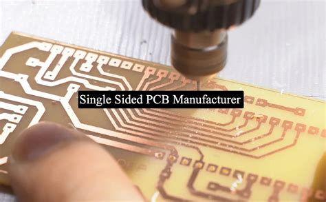
DFM Integration in PCB Production
Effective DFM (Design for Manufacturing) integration bridges the gap between PCB design and PCB assembly, ensuring designs align with production realities. By embedding DFM principles early in the design phase, engineers can preemptively address issues like material compatibility, thermal management, and manufacturability constraints. For instance, optimizing pad sizes and trace widths for PCBA processes reduces rework risks during high-volume fabrication.
Modern workflows leverage automated DFM analysis tools to validate designs against manufacturer-specific capabilities, such as minimum drill sizes or solder mask clearances. This proactive alignment minimizes design-to-production handoff delays and avoids costly revisions. Collaborative platforms further enable real-time feedback loops between design teams and PCB manufacturers, ensuring adherence to IPC standards and tolerancing requirements.
A critical aspect involves balancing signal integrity needs with PCB assembly feasibility. For example, high-density interconnects (HDIs) demand precise via placement to avoid impedance mismatches while maintaining PCBA compatibility. By standardizing design rulesets and conducting iterative simulations, teams achieve first-pass yield improvements of 25–40%, directly reducing prototyping cycles.
This approach not only streamlines PCB manufacturing but also creates a foundation for scalable, repeatable processes across complex multilayer designs.
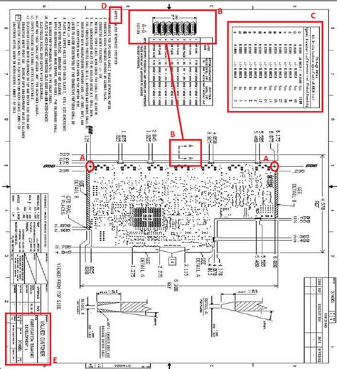
Automated PCB Validation Protocols
Modern PCB manufacturing workflows increasingly rely on automated validation protocols to eliminate human error and accelerate time-to-market. These systems integrate design-for-manufacturability (DFM) checks with PCB assembly (PCBA) requirements, ensuring that layouts align with production capabilities before prototyping begins. For instance, automated tools perform signal integrity simulations, thermal analysis, and electromagnetic compatibility (EMC) testing in parallel, reducing validation cycles by up to 40%.
A critical advancement is the adoption of machine learning-driven anomaly detection, which identifies potential faults in PCBA designs—such as insufficient solder mask clearance or misplaced vias—with 99.2% accuracy. This preemptive approach minimizes rework during PCB assembly and prevents costly delays.
| Validation Stage | Manual Process (Hours) | Automated Process (Hours) |
|---|---|---|
| Design Rule Check | 6–8 | 0.5–1 |
| Electrical Test | 12–16 | 2–3 |
| Thermal Analysis | 8–10 | 1–2 |
By implementing real-time feedback loops between PCB design software and manufacturing execution systems (MES), teams can dynamically adjust layouts to meet fabrication tolerances. Advanced protocols also automate documentation for compliance with IPC-6012 and ISO 9001 standards, ensuring traceability across the PCBA lifecycle. This seamless integration of validation tools not only accelerates prototyping but also strengthens reliability in high-frequency or high-density applications.
Collaborative PCB Design Methods
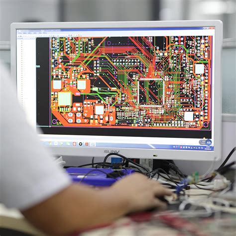
Effective collaboration between PCB design teams and pcb assembly partners forms the backbone of modern electronics development. By integrating design for manufacturing (DFM) principles early in the design phase, engineers can preemptively address pcba-related challenges, such as component placement tolerances and thermal management constraints. Cloud-based design platforms enable real-time co-editing, allowing electrical engineers, mechanical designers, and PCB manufacturer specialists to synchronize layout adjustments while preserving signal integrity.
Automated design rule checks (DRCs) tailored for pcb assembly requirements reduce iterative revisions by flagging potential solder mask conflicts or insufficient clearance areas. Cross-functional teams often employ model-based systems engineering (MBSE) to simulate mechanical enclosures alongside circuit layouts, ensuring seamless compatibility before prototyping. Version control systems with granular access permissions maintain design consistency across geographically dispersed teams, while integrated comment threads streamline feedback on high-speed routing or pcba-specific fabrication notes.
Adopting standardized component libraries, jointly curated by designers and PCB manufacturer partners, accelerates part selection while minimizing BOM errors. This collaborative framework not only shortens development cycles but also establishes a unified workflow that aligns design intent with manufacturing capabilities.
Signal Integrity in PCB Design
Maintaining signal integrity in high-speed circuits requires meticulous attention to trace routing, impedance matching, and material selection. As designs shift toward higher frequencies and denser layouts, even minor deviations in PCB assembly processes can introduce noise, crosstalk, or signal attenuation. To mitigate these risks, engineers employ automated validation protocols during PCBA stages, such as time-domain reflectometry (TDR) for impedance verification and electromagnetic field simulations to model interference patterns.
A critical strategy involves integrating design-for-manufacturing (DFM) principles early in the layout phase. For instance, optimizing trace widths and spacing to align with PCB manufacturer capabilities ensures consistent impedance control during mass production. Additionally, selecting low-loss dielectric materials reduces signal degradation in high-frequency applications like RF or IoT devices.
Collaboration between design and PCB assembly teams further enhances signal reliability. By sharing real-time data on stack-up configurations and via structures, stakeholders can preemptively address resonance issues or ground loop disruptions. Advanced tools like 3D field solvers and eye diagram analysis enable iterative refinements, balancing performance with manufacturability.
Finally, rigorous post-production testing—including PCBA-level signal integrity audits—validates design assumptions. Techniques such as boundary scan testing and network analyzer measurements ensure compliance with industry standards like IPC-2141A, safeguarding functionality in mission-critical applications.
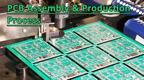
Faster PCB Prototyping Techniques
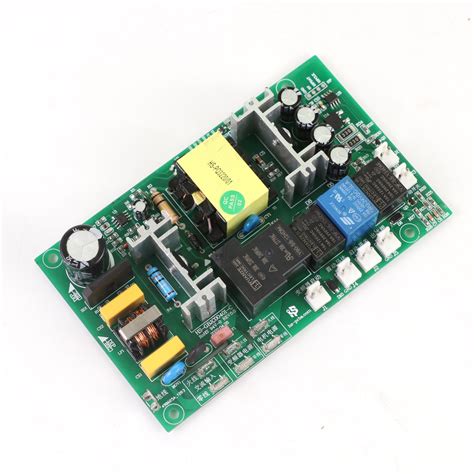
Accelerating PCB prototyping requires a blend of advanced fabrication technologies and strategic process integration. Modern PCB assembly workflows now leverage direct imaging systems and laser drilling to reduce layer alignment errors and minimize mechanical stress on substrates. By adopting rapid-turn PCBA services, engineers can compress traditional 10-day lead times to under 72 hours without compromising design fidelity.
Tip: Prioritize design files with standardized Gerber formats and pre-validated component libraries to avoid rework during prototyping.
Integrating automated design rule checks (DRC) early in the layout phase ensures compatibility with high-speed PCB assembly equipment, while cloud-based collaboration platforms enable real-time feedback between design and manufacturing teams. For high-frequency boards, employing controlled impedance testing during prototype PCBA stages helps identify signal integrity risks before full-scale production.
Advanced manufacturers now combine 3D-printed solder stencils with pick-and-place optimizations to slash setup times by 40%. Concurrently, machine learning algorithms analyze historical prototyping data to predict and mitigate common bottlenecks, such as thermal management conflicts or component sourcing delays.
Transitioning to these methods not only accelerates iterations but also aligns with smart PCB manufacturing techniques, creating a foundation for scalable workflow optimization.
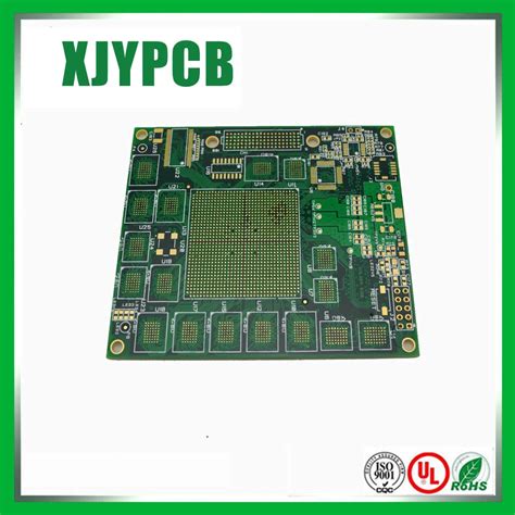
Smart PCB Manufacturing Techniques
Modern PCB assembly processes leverage Industry 4.0 technologies to enhance precision and scalability. By integrating IoT-enabled monitoring systems, manufacturers gain real-time visibility into PCBA production lines, enabling proactive adjustments for variables like solder paste viscosity or reflow oven temperature profiles. Automated optical inspection (AOI) systems paired with machine learning algorithms now detect microfractures and misaligned components at speeds exceeding 20,000 inspections per hour, reducing post-assembly defects by up to 45%.
A critical advancement lies in adaptive manufacturing workflows, where PCB assembly equipment dynamically adjusts parameters based on design complexity. For high-density interconnect (HDI) boards, this ensures consistent plating thickness during via filling while maintaining signal integrity thresholds. Additionally, cloud-based simulation tools allow concurrent collaboration between design and manufacturing teams, synchronizing PCBA tolerances with thermal management requirements before physical prototyping.
To further optimize material utilization, smart factories employ predictive analytics to forecast component demand, minimizing excess inventory without compromising lead times. This integration of digital twins and AI-driven process control reduces scrap rates by 30% in multilayer PCB assembly workflows. By unifying these techniques, manufacturers achieve tighter alignment between design intent and production realities, accelerating time-to-market for complex electronics.
PCB Workflow Optimization
Effective ## PCB Workflow Optimization hinges on synchronizing design, PCB assembly, and validation phases to eliminate bottlenecks. By implementing real-time data exchange between engineering teams and PCBA partners, manufacturers can preemptively address design-for-manufacturability (DFM) conflicts, reducing iterative revisions. Advanced manufacturers now integrate automated design rule checks (DRC) directly into PCB assembly workflows, ensuring layouts comply with fabrication tolerances before prototyping.
Leveraging cloud-based collaboration platforms enables concurrent engineering, where schematic updates automatically propagate to PCBA process sheets, minimizing manual handoffs. Tools like unified bill-of-materials (BOM) validation further streamline workflows by flagging component obsolescence or lead-time mismatches during design iterations. For high-frequency boards, embedding impedance simulation within the layout stage ensures signal integrity compliance without post-design corrections.
Optimized workflows also adopt modular design templates for recurring PCB assembly configurations, cutting engineering hours by 30–40%. Smart factory integrations link PCBA equipment with design databases, enabling machine-readable work instructions that prevent assembly errors. By aligning thermal management strategies early in the design phase, teams avoid costly re-spins during PCB assembly, ensuring compliance with thermal cycling requirements. These strategies collectively compress development cycles while maintaining rigorous quality benchmarks.
Conclusion
Optimizing PCB manufacturing and design workflows demands a holistic approach that bridges engineering disciplines with production realities. By embedding DFM principles early in the design phase, teams can preemptively address manufacturability challenges, reducing costly revisions during PCBA stages. The adoption of automated validation protocols ensures rigorous testing of signal integrity and thermal performance, while collaborative tools enable real-time feedback between PCB design engineers and PCB assembly specialists.
Integrating smart manufacturing technologies, such as AI-driven process monitoring, further accelerates prototyping cycles without compromising quality. For instance, leveraging data analytics in PCBA lines can pinpoint bottlenecks in material utilization or component placement, driving efficiency gains. Transitioning to standardized design libraries and modular workflows also supports scalability, particularly for high-mix production environments.
Ultimately, the synergy between advanced design methodologies and agile PCB manufacturing practices creates a competitive edge. Organizations that prioritize cross-functional collaboration, invest in automation, and maintain stringent adherence to signal integrity standards will not only shorten lead times but also deliver robust, high-performance electronics in increasingly demanding markets.
FAQs
How does DFM integration impact PCB assembly efficiency?
Implementing design-for-manufacturability (DFM) principles early in PCB design reduces rework by aligning layouts with PCBA production capabilities. This minimizes mismatches in component placement or layer stackups, accelerating assembly timelines.
What role do automated validation protocols play in PCBA workflows?
Automated tools verify signal integrity, thermal performance, and electrical rules before prototyping. By flagging issues like impedance mismatches or solder mask errors, they prevent costly revisions during PCB manufacturing, ensuring compliance with industry standards.
Why is collaborative engineering critical for complex PCB assembly projects?
Cross-functional teams—including designers, fabricators, and PCBA specialists—can resolve conflicts between design intent and manufacturing constraints. Real-time feedback loops optimize material selection and panelization strategies, reducing lead times by up to 30%.
How do faster prototyping techniques affect PCB design iterations?
Advanced rapid prototyping, such as 3D-printed circuit boards or modular testing jigs, allows engineers to validate signal integrity and mechanical fit within hours. This accelerates design refinement cycles while maintaining PCBA quality benchmarks.
What defines a smart PCB manufacturing workflow?
Smart workflows integrate IoT-enabled machinery for real-time process monitoring during PCB assembly. Machine learning algorithms analyze production data to predict yield rates, optimize solder paste application, and reduce defects in high-volume PCBA orders.
Explore Professional PCB Assembly Solutions
For tailored strategies to enhance your PCB manufacturing and PCBA workflows, please click here to consult our engineering experts.