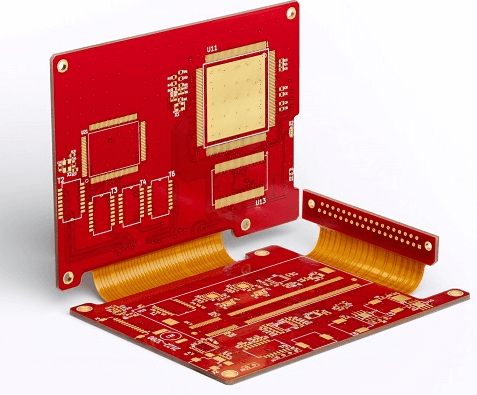
Pcb manufacturing requirements
Essential Materials For PCB Manufacturing
Printed Circuit Boards (PCBs) are the backbone of modern electronic devices, serving as the foundation upon which electronic components are mounted and interconnected. The manufacturing of PCBs requires a meticulous selection of materials to ensure functionality, reliability, and durability. Understanding the essential materials involved in PCB manufacturing is crucial for producing high-quality boards that meet industry standards.
To begin with, the substrate material forms the base of the PCB and is typically made from fiberglass-reinforced epoxy resin, known as FR-4.
This material is favored for its excellent mechanical strength, thermal stability, and electrical insulation properties. The choice of substrate is critical as it must withstand the thermal and mechanical stresses encountered during both the manufacturing process and the operational life of the PCB. Alternatives to FR-4, such as polyimide or ceramic substrates, may be used in applications requiring higher temperature resistance or specific electrical characteristics.
Next, the conductive material, usually copper, is essential for creating the electrical pathways on the PCB.
Copper is chosen for its superior electrical conductivity and ease of etching, which allows for precise patterning of the circuit traces. The copper is typically laminated onto the substrate in thin sheets, and its thickness can vary depending on the current-carrying requirements of the circuit. Standard copper thicknesses are measured in ounces per square foot, with common values being 1 oz/ft², 2 oz/ft², and 3 oz/ft².
In addition to the substrate and conductive materials, the solder mask is another critical component in PCB manufacturing.
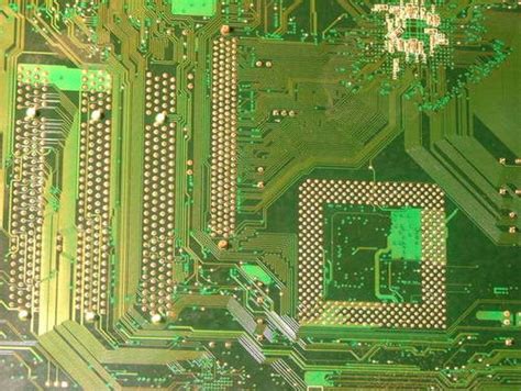
The solder mask is a protective layer applied over the copper traces to prevent short circuits and corrosion. It also helps to define the areas where solder should be applied during the component assembly process. The solder mask is usually made from a polymer-based material and is available in various colors, with green being the most common due to its optimal contrast for visual inspection.
Furthermore, the silkscreen layer is used to print text and symbols on the PCB, providing valuable information such as component labels, part numbers, and manufacturer logos.
The silkscreen is typically applied using a non-conductive ink, which must be resistant to the soldering process and other environmental factors. White is the most commonly used color for silkscreen, as it offers high visibility against the green solder mask.
Another essential material in PCB manufacturing is the surface finish, which is applied to the exposed copper areas to protect them from oxidation and ensure good solderability. Various surface finishes are available, each with its advantages and limitations. Common finishes include Hot Air Solder Leveling (HASL), Electroless Nickel Immersion Gold (ENIG), and Organic Solderability Preservative (OSP). The choice of surface finish depends on factors such as cost, shelf life, and the specific requirements of the end application.
Lastly, the use of adhesives and bonding materials is crucial in multilayer PCB manufacturing.
These materials are used to bond the individual layers of the PCB together, ensuring structural integrity and reliable electrical performance. Prepreg, a fiberglass cloth impregnated with resin, is commonly used for this purpose. The prepreg layers are stacked between the copper-clad laminates and subjected to heat and pressure to form a solid, unified board.
In conclusion, the selection of materials in PCB manufacturing is a complex process that requires careful consideration of various factors to ensure the production of high-quality, reliable PCBs. From the substrate and conductive materials to the solder mask, silkscreen, surface finish, and adhesives, each material plays a vital role in the overall performance and longevity of the final product. Understanding these essential materials and their properties is fundamental for anyone involved in the design and manufacturing of PCBs.
Key Design Rules For PCB Fabrication
Printed Circuit Board (PCB) manufacturing is a complex process that requires adherence to specific design rules to ensure functionality, reliability, and manufacturability. These design rules are critical as they guide the layout and fabrication of PCBs, ensuring that the final product meets the necessary standards and performs as intended. One of the primary considerations in PCB design is the trace width. The trace width must be carefully calculated based on the current-carrying capacity required for the circuit. Insufficient trace width can lead to overheating and potential failure of the PCB. Therefore, designers must refer to IPC-2221 standards, which provide guidelines on the appropriate trace width for different current levels.
Another crucial aspect is the spacing between traces. Adequate spacing is essential to prevent electrical shorts and ensure signal integrity.
The minimum spacing is typically determined by the voltage levels in the circuit and the manufacturing capabilities of the PCB fabricator. High-density designs, such as those found in modern electronics, often require very fine spacing, which can be challenging to achieve without advanced manufacturing techniques. Consequently, designers must collaborate closely with fabricators to understand their capabilities and limitations.
The choice of materials also plays a significant role in PCB fabrication.
The substrate material, usually FR4, must be selected based on the thermal, electrical, and mechanical requirements of the application. High-frequency circuits, for instance, may require materials with lower dielectric constants to minimize signal loss. Additionally, the copper thickness on the PCB must be specified according to the current requirements and thermal management needs. Thicker copper layers can handle higher currents but may also increase the cost and complexity of the manufacturing process.
Via design is another critical factor in PCB fabrication.
Vias are used to connect different layers of a PCB, and their size and placement must be carefully considered. Microvias, blind vias, and buried vias are commonly used in multi-layer PCBs to save space and improve performance. However, these types of vias require more advanced manufacturing processes and can increase the overall cost. Therefore, designers must balance the need for compactness with the constraints of the manufacturing process.
Thermal management is an often-overlooked aspect of PCB design but is crucial for the reliability and longevity of the final product.
Components that generate significant heat must be placed strategically to ensure efficient heat dissipation. Thermal vias, heat sinks, and proper trace layout can help manage heat effectively. Additionally, the PCB layout should facilitate adequate airflow if the board is to be used in an environment where active cooling is employed.
Signal integrity is another key consideration, especially in high-speed digital and RF circuits.
Impedance control, proper grounding, and minimizing electromagnetic interference (EMI) are essential to maintain signal quality. Designers must use techniques such as differential signaling, controlled impedance traces, and proper grounding schemes to mitigate signal integrity issues. Furthermore, the use of simulation tools can help identify potential problems early in the design phase, allowing for corrective measures before fabrication.
In conclusion, adhering to key design rules is essential for successful PCB fabrication. From trace width and spacing to material selection, via design, thermal management, and signal integrity, each aspect plays a vital role in ensuring that the final product meets the desired specifications. By understanding and implementing these design rules, designers can create PCBs that are not only functional and reliable but also manufacturable within the constraints of current technology.
Quality Control Measures In PCB Production
In the realm of printed circuit board (PCB) manufacturing, quality control measures are paramount to ensure the reliability and functionality of the final product. The intricate nature of PCBs, which serve as the backbone of virtually all electronic devices, necessitates rigorous quality control protocols throughout the production process. These measures are designed to detect and mitigate potential defects, ensuring that each PCB meets stringent industry standards and customer specifications.
To begin with, the initial stage of PCB production involves the careful selection of raw materials.
High-quality substrates, copper foils, and laminates are essential to the integrity of the final product. Suppliers are meticulously vetted, and materials are subjected to thorough inspections upon arrival. This preliminary step is crucial, as the use of substandard materials can lead to significant issues down the line, including delamination, warping, and electrical failures.
Following material selection, the design phase incorporates advanced software tools to simulate and verify the PCB layout.
Design for manufacturability (DFM) checks are conducted to identify potential issues that could arise during production. These checks include verifying trace widths, spacing, and hole sizes, as well as ensuring that the design adheres to the capabilities of the manufacturing equipment. By addressing these concerns early in the process, manufacturers can prevent costly errors and rework.
As the production process progresses to the fabrication stage, photolithography is employed to transfer the PCB design onto the substrate.
This step requires precise alignment and exposure to ultraviolet light to create the desired circuit patterns. Quality control measures at this stage include inspecting the photomasks for defects and ensuring that the exposure process is accurately calibrated. Any deviations can result in misaligned or incomplete circuits, compromising the functionality of the PCB.
Subsequently, the etching process removes unwanted copper, leaving behind the desired circuit traces.
This step is closely monitored to ensure that the etching solution is properly maintained and that the etching time is precisely controlled. Inadequate etching can lead to short circuits or open circuits, both of which can render the PCB unusable. Post-etching inspections, including automated optical inspection (AOI), are conducted to detect any defects in the circuit patterns.
Drilling and plating are critical steps that follow, involving the creation of vias and through-holes that connect different layers of the PCB.
Precision drilling equipment is used to achieve the required hole sizes and placements. The plating process, which deposits a thin layer of copper onto the hole walls, is carefully controlled to ensure uniform coverage. Quality control measures at this stage include inspecting the hole integrity and verifying the thickness of the copper plating.
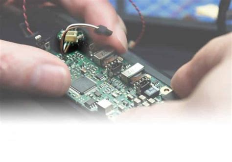
Finally, the assembly process involves the placement and soldering of electronic components onto the PCB.
Surface mount technology (SMT) and through-hole technology (THT) are commonly used methods. Quality control measures during assembly include solder paste inspection (SPI), AOI, and X-ray inspection to detect soldering defects such as insufficient solder, bridging, and voids. Functional testing is also performed to verify that the assembled PCB operates as intended.
In conclusion, quality control measures in PCB production are integral to ensuring the reliability and performance of the final product. From material selection and design verification to fabrication, assembly, and testing, each stage of the production process incorporates rigorous inspections and controls. By adhering to these stringent quality control protocols, manufacturers can deliver PCBs that meet the highest standards of excellence, thereby supporting the continued advancement of electronic technology.
Environmental Regulations In PCB Manufacturing
The manufacturing of printed circuit boards (PCBs) is a complex process that involves various stages, each with its own set of environmental implications. As the demand for electronic devices continues to surge, the environmental regulations governing PCB manufacturing have become increasingly stringent. These regulations are designed to mitigate the environmental impact of the manufacturing process, ensuring that it is conducted in a manner that is both sustainable and responsible.
One of the primary environmental concerns in PCB manufacturing is the use of hazardous chemicals.
The etching process, for instance, often involves the use of strong acids and bases, which can be harmful if not properly managed. To address this, regulatory bodies have established guidelines for the safe handling, storage, and disposal of these chemicals. Compliance with these guidelines is not only a legal requirement but also a critical component of a company’s environmental stewardship.
In addition to chemical management, waste generation is another significant issue in PCB manufacturing.
The production process generates various types of waste, including solid waste, wastewater, and air emissions. Regulatory frameworks such as the Resource Conservation and Recovery Act (RCRA) in the United States mandate that manufacturers implement waste minimization strategies. These strategies may include recycling and reusing materials, as well as adopting cleaner production techniques that reduce the overall volume of waste generated.
Water usage and contamination are also critical areas of concern.
PCB manufacturing processes often require large quantities of water for rinsing and cleaning. The discharge of contaminated water can have detrimental effects on local water bodies and ecosystems. Consequently, regulations such as the Clean Water Act (CWA) in the United States require manufacturers to treat wastewater to remove harmful contaminants before it is discharged. This often involves the use of advanced treatment technologies, such as filtration and chemical neutralization, to ensure that the water meets stringent quality standards.
Air quality is another important aspect of environmental regulation in PCB manufacturing.
The use of volatile organic compounds (VOCs) and other airborne pollutants can contribute to air pollution and pose health risks to workers and nearby communities. Regulations such as the Clean Air Act (CAA) in the United States set limits on the emissions of these pollutants. Manufacturers are required to implement control measures, such as the use of scrubbers and filters, to capture and reduce emissions. Additionally, regular monitoring and reporting are mandated to ensure compliance with air quality standards.
Energy consumption is yet another factor that has garnered attention in recent years.
The energy-intensive nature of PCB manufacturing processes contributes to greenhouse gas emissions and climate change. Regulatory initiatives and industry standards now encourage manufacturers to adopt energy-efficient practices and technologies. This may include the use of renewable energy sources, energy-efficient equipment, and process optimization techniques to reduce overall energy consumption.
Furthermore, the global nature of the electronics industry means that PCB manufacturers must navigate a complex web of international regulations.
The European Union’s Restriction of Hazardous Substances (RoHS) directive, for example, restricts the use of certain hazardous materials in electronic products. Compliance with such regulations requires manufacturers to conduct thorough material assessments and implement robust supply chain management practices.
In conclusion, environmental regulations in PCB manufacturing are multifaceted and encompass various aspects of the production process. From chemical management and waste reduction to water treatment and air quality control, these regulations are designed to minimize the environmental impact of PCB manufacturing. Compliance with these regulations not only ensures legal adherence but also promotes sustainable practices that benefit both the environment and society at large. As the industry continues to evolve, ongoing efforts to enhance environmental performance will remain a critical priority for PCB manufacturers worldwide.