PCB Milling: A Comprehensive Guide to Rapid Prototyping of Printed Circuit Boards
Introduction to PCB Milling
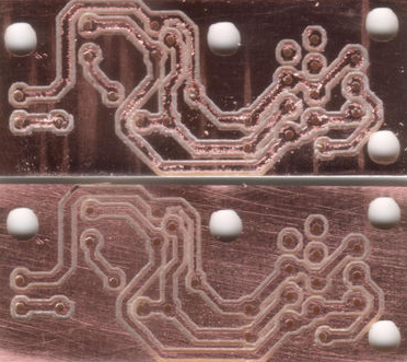
Printed Circuit Board (PCB) milling is a subtractive manufacturing process that uses computer-controlled milling machines to remove copper from a substrate to create electrical pathways and pads. This method has gained significant popularity among engineers, hobbyists, and small-scale manufacturers as an efficient alternative to traditional PCB fabrication methods like chemical etching.
Unlike chemical processes that require hazardous materials and produce toxic waste, PCB milling is a clean, dry process that can be performed in any laboratory or workshop environment. The technology enables rapid prototyping, allowing designers to go from concept to physical board in a matter of hours rather than days or weeks required for outsourced PCB fabrication.
How PCB Milling Works
The Basic Process
PCB milling follows a straightforward workflow:
- Design Creation: The circuit is designed using Electronic Design Automation (EDA) software, resulting in Gerber files or other standard PCB file formats.
- File Conversion: The design files are converted into toolpaths using specialized PCB milling software.
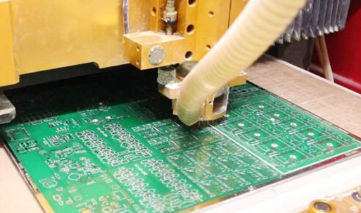
- Machine Setup: The copper-clad board is secured to the milling machine’s bed, and the appropriate milling bits are installed.
- Milling Operation: The machine precisely removes copper according to the design, creating isolation channels between traces.
- Drilling: Holes for through-hole components and vias are drilled using specialized drill bits.
- Finishing: The board is cleaned and optionally treated with protective coatings.
Key Components of a PCB Milling Machine
- Frame and Motion System: Typically uses linear guides or rods with stepper motors for precise X-Y-Z movement.
- Spindle: The rotating component that holds and drives the milling bits, usually ranging from 10,000 to 60,000 RPM.
- Control Electronics: Includes motor drivers, power supplies, and a controller (often running GRBL or similar firmware).
- Bed: A flat, stable surface for holding the workpiece, often with vacuum systems or mechanical clamps.
- Dust Collection: Many systems include vacuum systems to remove copper and substrate debris.
Advantages of PCB Milling
Rapid Prototyping Capabilities
PCB milling shines in rapid prototyping scenarios where design iterations are frequent. Engineers can:
- Make design changes and produce a new board in hours
- Test physical prototypes the same day they’re designed
- Implement immediate modifications based on test results
- Reduce development cycles from weeks to days
Environmental Benefits
Compared to chemical etching, PCB milling offers significant environmental advantages:
- No toxic chemicals (ferric chloride, ammonium persulfate, etc.)
- No liquid waste requiring special disposal
- Minimal material waste (only the removed copper is discarded)
- Lower energy consumption compared to industrial PCB processes
Design Flexibility
Milling provides unique design capabilities:
- Immediate modification of trace widths and spacing
- Ability to create non-standard board shapes and cutouts
- Option to mill solder masks and legend layers
- Capability to produce RF/microwave circuits with precise impedance control
- Flexibility to work with various substrate materials
Cost Effectiveness for Small Runs
For small quantities (1-10 boards), milling is often more economical than outsourcing:
- No minimum order quantities
- No shipping costs or delays
- No tooling or setup fees
- Low material costs (standard copper-clad boards)
- Reusable substrates for experimental designs
Technical Considerations in PCB Milling
Tool Selection
Choosing the right milling bits is crucial for quality results:
- End Mills for Trace Isolation: Typically 10° to 30° V-bits with diameters from 0.1mm to 0.3mm
- Drill Bits: Standard PCB drill sizes from 0.3mm to 2.0mm for component holes
- Cutout Tools: Larger end mills (1-3mm) for board outlines and large clearance areas
Material Considerations
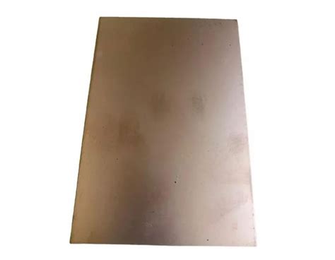
PCB milling works with various substrate materials:
- FR-4: Standard fiberglass epoxy, most common for rigid PCBs
- RF Materials: Rogers, PTFE, and other high-frequency substrates
- Flexible Circuits: Polyimide films with thin copper layers
- Aluminum Backed: For heat dissipation applications
Design Rules for Milled PCBs
Successful milling requires adherence to specific design constraints:
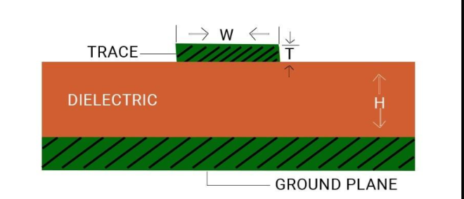
- Minimum Trace Width: Typically 0.2mm (8mil) for reliable milling
- Clearance: At least 0.2mm between traces
- Isolation Width: Minimum 0.3mm for V-bit milling
- Pad Sizes: Larger than chemically etched boards (minimum 0.5mm annular ring)
- Via Handling: Either drilled as through-holes or designed for manual insertion
Software Workflow
The typical software chain includes:
- EDA Tools: KiCad, Eagle, Altium Designer, OrCAD
- CAM Processors: FlatCAM, OpenBuilds CAM, commercial PCB milling software
- Machine Control: Universal G-code Sender, Mach3, proprietary controllers
Limitations and Challenges
While powerful, PCB milling has some inherent limitations:
- Resolution Limits: Cannot achieve the fine traces/spacing of professional PCBs (typically limited to ~6mil traces)
- Through-Plating: Cannot create plated through-holes without additional processes
- Multi-Layer Complexity: Limited to 1-2 layers practically (4 layers possible with advanced alignment)
- Surface Finish: Exposed copper requires protection against oxidation
- Time Intensive: Larger boards or complex designs can take hours to mill
Advanced Techniques
Double-Sided PCB Milling
Creating double-sided boards requires precise alignment:
- Fiducial Markers: Milled alignment holes used for flipping the board
- Pin Alignment Systems: Mechanical alignment using tooling pins
- Optical Alignment: Camera systems for precise registration
Solder Mask Application
Post-milling processes can enhance board quality:
- LPI Solder Mask: Liquid photoimageable mask applied and cured
- Dry Film: Laminate solder mask material
- Inkjet Printing: Direct application of mask materials
Surface Finishes
Options for protecting exposed copper:
- ENIG (Electroless Nickel Immersion Gold): Requires chemical process
- Immersion Silver: Simple dip process
- OSP (Organic Solderability Preservative): Temporary protective coating
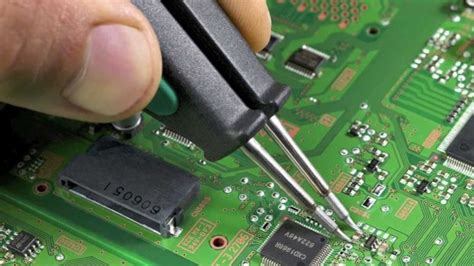
- Hand Soldering: Manual tinning of traces
Comparison with Alternative Prototyping Methods
PCB Milling vs. Chemical Etching
| Factor | PCB Milling | Chemical Etching |
|---|---|---|
| Speed | Moderate (minutes to hours) | Fast (10-30 minutes active time) |
| Resolution | Good (6-10mil typical) | Excellent (3-5mil possible) |
| Safety | Very safe | Hazardous chemicals |
| Environment | Clean, no waste | Toxic waste disposal |
| Setup | Machine required | Chemical tanks needed |
| Cost per board | Moderate | Low |
| Double-sided | Possible with alignment | Easier alignment |
PCB Milling vs. Professional PCB Fabrication
| Factor | PCB Milling | Professional Fabrication |
|---|---|---|
| Lead Time | Hours | Days to weeks |
| Cost (small qty) | Low | Moderate to high |
| Cost (large qty) | High | Very low |
| Layer Count | 1-2 (4 possible) | Up to 30+ layers |
| Feature Size | 6mil+ | 3mil+ |
| Through-Plating | No | Yes |
| Solder Mask | Optional | Standard |
| Silkscreen | Optional | Standard |
Future Developments in PCB Milling Technology
The field continues to evolve with several promising directions:
- Higher Precision Spindles: Enabling finer traces and smaller vias
- Laser Hybrid Systems: Combining milling with laser for finer features
- Automated Tool Changers: Reducing manual intervention in the milling process
- Improved Software: Better design rule checking and toolpath optimization
- Additive Hybrid Approaches: Combining subtractive milling with conductive ink printing
- In-Situ Inspection: Integrated cameras and probes for quality verification
Practical Applications
PCB milling finds use in numerous scenarios:
- University Labs: For teaching electronics and rapid project development
- Research Institutions: Fast iteration on experimental circuits
- Startups: Cost-effective prototyping before production runs
- Hobbyists: Home electronics projects and custom devices
- Field Repairs: Creating replacement boards or patches for equipment
- Specialty Electronics: RF, microwave, and high-voltage applications requiring custom geometries
Best Practices for Quality Results
To achieve professional-quality milled PCBs:
- Proper Machine Calibration: Regular checks of axis alignment and spindle runout
- Optimal Feed Rates: Balancing speed and quality (typically 50-150mm/s)
- Depth Control: Precise control of milling depth to avoid substrate damage
- Tool Maintenance: Regular inspection and replacement of worn bits
- Material Preparation: Secure, flat mounting of copper-clad boards
- Dust Management: Effective removal of milling debris
- Test Cuts: Verifying settings on scrap material before final boards
Conclusion
PCB milling represents a powerful tool in the electronics designer’s arsenal, offering unparalleled flexibility and speed for prototyping applications. While it may not replace professional PCB fabrication for final production, its advantages in rapid iteration, environmental friendliness, and small-batch economics make it indispensable for many development scenarios.
As the technology continues to advance, with improvements in precision, automation, and software integration, PCB milling is becoming accessible to an ever-wider range of users—from professional engineers to electronics enthusiasts. By understanding its capabilities and limitations, and following best practices in design and operation, users can reliably produce high-quality prototype PCBs that accelerate the development process and bring electronic concepts to reality with unprecedented speed.
The future of PCB milling looks bright, with emerging technologies promising to bridge the gap between prototype and production quality, potentially revolutionizing how small-to-medium volume electronic products are developed and manufactured. As these trends continue, PCB milling will likely become an even more essential capability for electronics development across all sectors.