PCB Package Design: A Comprehensive Guide
Introduction to PCB Package Design
Printed Circuit Board (PCB) package design is a critical aspect of electronic product development that bridges the gap between integrated circuit (IC) design and physical implementation. This specialized field involves creating the physical housing and interconnection system that allows semiconductor devices to interface with the rest of the electronic system. Effective PCB package design ensures signal integrity, power delivery, thermal management, and mechanical stability while meeting increasingly demanding performance requirements in smaller form factors.
As electronic devices continue to shrink in size while growing in complexity, the importance of proper PCB package design has never been greater. Modern packages must accommodate higher pin counts, faster signal speeds, and greater power densities while maintaining reliability and manufacturability. This article explores the fundamental principles, key considerations, and current trends in PCB package design.
Fundamentals of PCB Package Design
Package Types and Classifications
PCB packages come in various forms, each suited to specific applications and requirements:
- Through-Hole Packages: The traditional packaging method where leads are inserted into holes drilled in the PCB (e.g., DIP, PGA)
- Surface Mount Packages: Modern packages that mount directly onto PCB surfaces (e.g., QFP, BGA, LGA)
- Chip-Scale Packages (CSP): Packages that are no more than 1.2 times the size of the die itself
- Ball Grid Array (BGA): High-density packages with solder balls arranged in a grid pattern underneath
- Quad Flat Packages (QFP): Packages with leads extending from all four sides
- Land Grid Array (LGA): Similar to BGA but with flat contacts instead of solder balls
Key Design Elements
Every PCB package design must address several fundamental elements:
- Die Attachment: The method of connecting the semiconductor die to the package substrate
- Interconnection: The system that connects the die to the package pins (wire bonding, flip-chip, etc.)
- Leadframe/Substrate: The structural foundation that provides mechanical support and electrical pathways
- Encapsulation: The protective material that surrounds the die (typically epoxy molding compound)
- Thermal Management: Features designed to dissipate heat from the die
Design Considerations and Challenges
Signal Integrity
Maintaining signal integrity becomes increasingly challenging as clock speeds rise and form factors shrink. Key considerations include:
- Impedance Control: Matching impedance throughout the signal path to minimize reflections
- Crosstalk Mitigation: Proper spacing and shielding to prevent interference between signals
- Return Path Design: Ensuring clean reference planes for high-speed signals
- Via Optimization: Minimizing via stub lengths and using appropriate via structures
Power Delivery
Modern ICs require stable power with low noise, presenting several design challenges:
- Power Integrity: Maintaining stable voltage levels despite varying current demands
- Decoupling Strategy: Proper placement and selection of decoupling capacitors
- Power Plane Design: Optimizing plane shapes and splits for minimal impedance
- Current Carrying Capacity: Ensuring traces and planes can handle required currents
Thermal Management
As power densities increase, thermal considerations become paramount:
- Thermal Interface Materials: Selecting appropriate materials between die and heat spreader
- Heat Spreader Design: Optimizing materials and geometry for heat dissipation
- Thermal Vias: Implementing via arrays under hot components
- Airflow Considerations: Designing packages to work with system-level cooling solutions
Manufacturability and Reliability
The design must be producible and reliable throughout its lifecycle:
- Design for Manufacturing (DFM): Ensuring the design can be reliably produced
- Design for Test (DFT): Incorporating features for production testing
- Mechanical Stress Management: Accounting for thermal expansion mismatches
- Environmental Protection: Ensuring resistance to moisture, contaminants, etc.
PCB Package Design Process
1. Requirements Definition
The design process begins with clearly defining requirements:
- Electrical performance specifications
- Physical size constraints
- Thermal requirements
- Environmental conditions
- Cost targets
- Reliability expectations
2. Package Selection
Based on requirements, select an appropriate package type considering:
- Pin count and density
- Performance characteristics
- Thermal needs
- Assembly processes
- Availability and cost
3. Substrate Design
The substrate design includes:
- Layer stackup definition
- Trace routing and spacing
- Via selection and placement
- Power and ground distribution
- Impedance control structures
4. Thermal Design
Thermal management features are incorporated:
- Heat spreader design
- Thermal via placement
- Interface material selection
- Airflow considerations
5. Mechanical Design
Physical aspects are finalized:
- Package dimensions and tolerances
- Lead/ball arrangement
- Mounting features
- Marking and labeling
6. Verification and Validation
The design undergoes rigorous checking:
- Electrical rule checking (ERC)
- Design rule checking (DRC)
- Signal integrity analysis
- Power integrity analysis
- Thermal analysis
- Mechanical stress analysis
Advanced Topics in PCB Package Design
High-Density Interconnect (HDI)
HDI technologies enable finer features and higher densities:
- Microvias and buried vias
- Finer trace/space capabilities
- Sequential lamination processes
- Advanced materials with better dimensional stability
3D Packaging
Emerging technologies that stack components vertically:
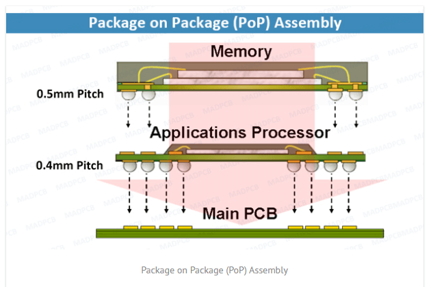
- Package-on-package (PoP)
- Through-silicon vias (TSVs)
- Silicon interposers
- Fan-out wafer-level packaging (FOWLP)
RF and Microwave Packaging
Special considerations for high-frequency applications:
- Controlled impedance structures
- Shielding and isolation techniques
- Low-loss material selection
- Antenna integration
Flexible and Stretchable Electronics
Packaging for non-traditional applications:
- Flexible substrates
- Stretchable interconnects
- Conformal packaging
- Novel encapsulation methods
Tools and Technologies for PCB Package Design
Modern PCB package design relies on sophisticated software tools:
- EDA Tools: Cadence Allegro, Mentor Xpedition, Altium Designer
- Simulation Software: ANSYS HFSS, SIwave, Cadence Sigrity
- Thermal Analysis Tools: FloTHERM, Icepak
- Mechanical CAD: SolidWorks, Autodesk Inventor
- DFM/DFA Tools: Valor NPI, CAM350
These tools enable complex multi-physics simulations that predict electrical, thermal, and mechanical performance before physical prototyping.
Future Trends in PCB Package Design
The field continues to evolve with several emerging trends:
- Heterogeneous Integration: Combining disparate technologies in single packages
- Chiplet Architectures: Modular IC designs with separate packaged elements
- Advanced Materials: Nanomaterials, 2D materials, and novel composites
- Embedded Components: Passive and active components within the substrate
- Sustainable Packaging: Eco-friendly materials and manufacturing processes
- AI-Assisted Design: Machine learning for design optimization
Conclusion
PCB package design represents a critical intersection of electrical, mechanical, thermal, and materials engineering. As electronic systems grow more complex while shrinking in size, the importance of proper package design only increases. Successful package designers must balance competing requirements while considering the entire product lifecycle from manufacturing to end-use.
The field continues to evolve rapidly, with new materials, processes, and architectures emerging to meet the demands of next-generation electronics. Staying current with these developments while maintaining a solid foundation in fundamental principles is key to successful PCB package design.
By understanding the comprehensive aspects covered in this article—from basic package types to advanced integration techniques—designers can create robust, high-performance packaging solutions that enable the electronic devices of today and tomorrow.


