PCB Population: A Comprehensive Guide
Introduction
Printed Circuit Boards (PCBs) are the backbone of modern electronics. They provide the necessary platform for mounting and interconnecting electronic components to create functional circuits. The process of populating a PCB, often referred to as PCB assembly or PCB population, involves placing and soldering electronic components onto the board. This article delves into the various aspects of PCB population, including the methods, technologies, challenges, and best practices involved in the process.
1. Understanding PCB Population
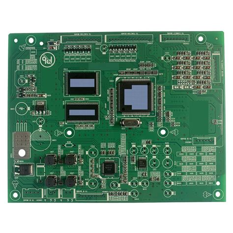
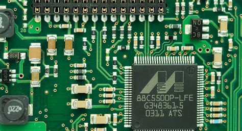
PCB population is the process of assembling electronic components onto a PCB to create a functional electronic device. This process can be done manually or through automated methods, depending on the complexity of the design, the volume of production, and the type of components used.
1.1. Types of PCB Population
There are two primary methods of PCB population:
- Through-Hole Technology (THT): In this method, components with leads are inserted into pre-drilled holes on the PCB and soldered onto pads on the opposite side. THT is known for its strong mechanical bonds, making it suitable for components that require high reliability and durability, such as connectors and large capacitors.
- Surface Mount Technology (SMT): SMT involves placing components directly onto the surface of the PCB. The components are then soldered onto pads using reflow soldering. SMT is widely used in modern electronics due to its ability to accommodate smaller components and higher component density, leading to more compact and lightweight designs.
1.2. Components Used in PCB Population
The components used in PCB population can be broadly categorized into active and passive components:
- Active Components: These include transistors, integrated circuits (ICs), microcontrollers, and other components that require a power source to function. Active components are essential for processing and controlling electrical signals.
- Passive Components: These include resistors, capacitors, inductors, and other components that do not require a power source to function. Passive components are used for filtering, energy storage, and signal conditioning.
2. PCB Population Process
The PCB population process involves several steps, each of which must be carefully executed to ensure the quality and functionality of the final product.
2.1. Design and Preparation
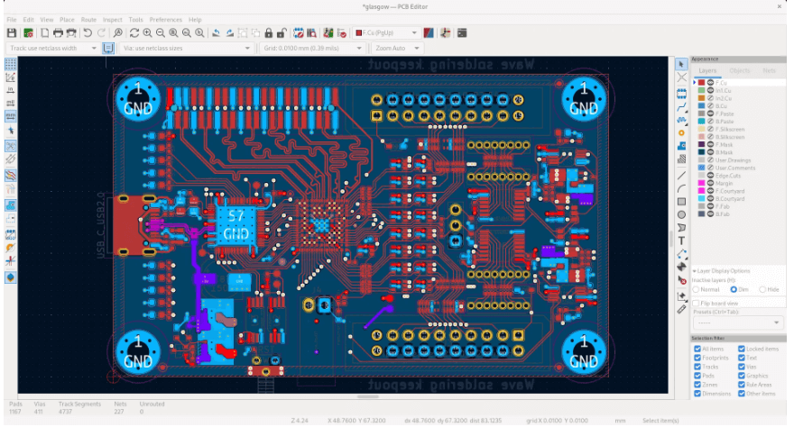
Before the actual population process begins, the PCB design must be finalized. This includes creating a schematic diagram, designing the PCB layout, and generating Gerber files, which are used by manufacturers to produce the PCB. The design must also include a Bill of Materials (BOM), which lists all the components required for the assembly.
2.2. Stencil Printing
In SMT, the first step in the population process is stencil printing. A stencil is used to apply solder paste onto the PCB pads where components will be placed. The solder paste is a mixture of tiny solder particles and flux, which helps the solder adhere to the pads and components during the reflow process.
2.3. Component Placement
Once the solder paste is applied, the next step is component placement. This can be done manually for low-volume production or prototypes, but for high-volume production, automated pick-and-place machines are used. These machines use vacuum nozzles to pick up components from reels or trays and place them accurately onto the PCB.
2.4. Reflow Soldering
After component placement, the PCB is passed through a reflow oven. The oven heats the PCB to a temperature that melts the solder paste, creating a strong electrical and mechanical bond between the components and the PCB. The reflow process is carefully controlled to ensure that the solder melts uniformly and that the components are not damaged by excessive heat.
2.5. Inspection and Testing
Once the soldering process is complete, the PCB undergoes inspection and testing. Automated Optical Inspection (AOI) systems are used to check for defects such as misaligned components, solder bridges, and insufficient solder. Functional testing is also performed to ensure that the assembled PCB operates as intended.
2.6. Through-Hole Component Insertion
For PCBs that include through-hole components, these components are inserted after the SMT process. This can be done manually or using automated insertion machines. The through-hole components are then soldered using wave soldering or selective soldering techniques.
2.7. Cleaning and Finishing
After all components are soldered, the PCB is cleaned to remove any flux residue or contaminants. Depending on the application, the PCB may also undergo additional finishing processes, such as conformal coating, to protect it from environmental factors like moisture and dust.
3. Challenges in PCB Population
PCB population is a complex process that presents several challenges, particularly as electronic devices become more compact and complex.
3.1. Miniaturization
The trend towards smaller and more compact devices has led to the use of smaller components, such as 0201 and 01005 packages. These tiny components require precise placement and soldering, which can be challenging even for advanced pick-and-place machines.
3.2. High-Density Interconnects (HDI)
HDI PCBs, which feature finer traces and smaller vias, are increasingly used in high-performance electronics. The high density of interconnects makes it more difficult to ensure proper solder joint formation and electrical connectivity.
3.3. Mixed Technology Assemblies
Many modern PCBs use a combination of SMT and THT components. This mixed technology assembly requires careful planning and execution to ensure that both types of components are properly placed and soldered without interfering with each other.
3.4. Thermal Management
As electronic devices become more powerful, managing heat dissipation becomes a critical challenge. Components that generate significant heat, such as power transistors and processors, must be carefully placed and soldered to ensure adequate thermal management.
4. Best Practices in PCB Population
To overcome the challenges and ensure a successful PCB population process, several best practices should be followed.
4.1. Design for Manufacturability (DFM)
DFM involves designing the PCB with the manufacturing process in mind. This includes considering factors such as component placement, solderability, and thermal management during the design phase. DFM helps to minimize potential issues during the population process and improves the overall yield.
4.2. Accurate BOM Management
A comprehensive and accurate BOM is essential for successful PCB population. The BOM should include detailed information about each component, including part numbers, descriptions, and specifications. Any discrepancies in the BOM can lead to delays, increased costs, and potential defects in the final product.
4.3. Quality Control
Implementing rigorous quality control measures throughout the PCB population process is crucial. This includes regular inspections, testing, and verification at each stage of the assembly process. Automated inspection systems, such as AOI and X-ray inspection, can help to identify defects early and prevent them from propagating to subsequent stages.
4.4. Proper Handling and Storage of Components
Electronic components are sensitive to environmental factors such as moisture, static electricity, and temperature. Proper handling and storage of components are essential to prevent damage and ensure their reliability. Components should be stored in anti-static packaging and kept in controlled environments to avoid exposure to moisture and contaminants.
4.5. Continuous Improvement
The PCB population process should be continuously monitored and improved. This includes analyzing defect rates, identifying root causes of issues, and implementing corrective actions. Continuous improvement helps to optimize the process, reduce costs, and improve the quality of the final product.
5. Future Trends in PCB Population
As technology continues to evolve, the PCB population process is also expected to undergo significant changes.
5.1. Advanced Automation
The use of advanced automation technologies, such as robotics and artificial intelligence (AI), is expected to increase in PCB population. These technologies can improve the accuracy and efficiency of component placement, soldering, and inspection, leading to higher yields and lower production costs.
5.2. 3D Printing
3D printing, also known as additive manufacturing, is emerging as a potential game-changer in PCB population. 3D printing can be used to create complex PCB designs with embedded components, reducing the need for traditional assembly processes. This technology is still in its early stages but holds promise for the future of PCB manufacturing.
5.3. Flexible and Stretchable PCBs
The demand for flexible and stretchable PCBs is growing, particularly in wearable electronics and medical devices. These PCBs require specialized population techniques to accommodate their unique properties, such as flexibility and durability. As the technology matures, new methods for populating flexible and stretchable PCBs are expected to emerge.
5.4. Environmental Considerations
As environmental regulations become more stringent, the PCB population process will need to adapt to meet these requirements. This includes the use of lead-free solder, environmentally friendly cleaning agents, and recyclable materials. Manufacturers will also need to consider the environmental impact of their processes and strive to minimize waste and energy consumption.
Conclusion
PCB population is a critical process in the manufacturing of electronic devices. It involves the precise placement and soldering of components onto a PCB to create a functional circuit. The process can be complex and challenging, particularly as electronic devices become more compact and sophisticated. However, by following best practices and staying abreast of emerging trends, manufacturers can overcome these challenges and produce high-quality PCBs that meet the demands of modern electronics. As technology continues to evolve, the PCB population process will also continue to advance, leading to more efficient, reliable, and environmentally friendly manufacturing methods.
+

