Pcb prototype assembly
Understanding The Basics Of PCB Prototype Assembly
Printed Circuit Board (PCB) prototype assembly is a critical phase in the development of electronic devices, serving as a bridge between the design and mass production stages. Understanding the basics of PCB prototype assembly is essential for engineers and designers to ensure the functionality and reliability of their electronic products. This process involves several key steps, each of which plays a vital role in transforming a conceptual design into a tangible, working prototype.
Initially, the process begins with the design phase, where engineers use specialized software to create a schematic diagram of the circuit.
This schematic serves as a blueprint, detailing the electrical connections and components required for the PCB. Once the schematic is finalized, it is converted into a layout design, which specifies the physical placement of components and the routing of electrical traces on the board. This layout must be meticulously checked for errors, as any mistake at this stage can lead to costly revisions later in the process.
Following the design phase, the next step is the fabrication of the PCB itself.
This involves creating the physical board, typically made from a non-conductive substrate such as fiberglass, coated with a thin layer of conductive material, usually copper. The design layout is transferred onto the board using a photolithographic process, where ultraviolet light is used to etch the circuit pattern onto the copper layer. After etching, the board undergoes a series of chemical treatments to remove any excess copper, leaving only the desired circuit traces.
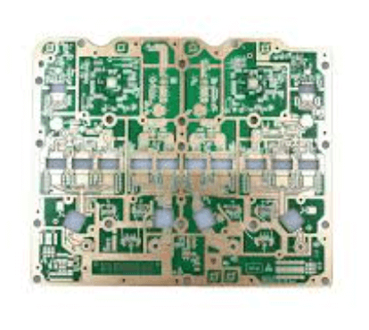
Once the PCB is fabricated, the assembly process begins.
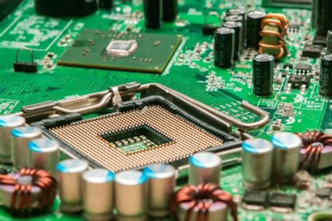
This involves placing and soldering electronic components onto the board according to the layout design. Components can be either surface-mounted or through-hole mounted, depending on the design specifications. Surface-mount technology (SMT) is commonly used for modern PCBs due to its efficiency and ability to accommodate smaller components. In contrast, through-hole technology involves inserting component leads into pre-drilled holes on the board and soldering them in place, providing a more robust mechanical connection.
To ensure the accuracy and reliability of the assembly, various inspection and testing procedures are employed.
Automated optical inspection (AOI) systems are used to verify the correct placement and orientation of components, while X-ray inspection can detect hidden defects such as solder joint issues. Functional testing is also conducted to ensure that the assembled PCB operates as intended. This may involve applying power to the board and running diagnostic tests to check for proper functionality and performance.
Throughout the PCB prototype assembly process, attention to detail and adherence to industry standards are paramount
. Any deviation from the design specifications or assembly procedures can result in a non-functional prototype, necessitating costly rework and delays. Therefore, collaboration between designers, engineers, and assembly technicians is crucial to ensure a successful outcome.
In conclusion, understanding the basics of PCB prototype assembly is fundamental for anyone involved in the development of electronic devices. From the initial design and layout to the fabrication and assembly stages, each step requires precision and expertise to produce a reliable and functional prototype. By adhering to best practices and employing rigorous inspection and testing methods, engineers can ensure that their PCB prototypes meet the necessary performance and quality standards, paving the way for successful mass production.
Top Challenges In PCB Prototype Assembly And How To Overcome Them
PCB prototype assembly is a critical phase in the development of electronic devices, serving as a bridge between design and mass production. However, this stage is fraught with numerous challenges that can impede progress and affect the final product’s quality. Understanding these challenges and implementing effective strategies to overcome them is essential for ensuring a smooth and successful assembly process.
One of the foremost challenges in PCB prototype assembly is the complexity of design.
Modern electronic devices demand intricate and compact designs, which can be difficult to translate into a functional prototype. This complexity often leads to issues such as signal interference, thermal management problems, and mechanical stress. To mitigate these issues, it is crucial to employ advanced design software that can simulate various scenarios and identify potential problems before the physical assembly begins. Additionally, collaborating closely with experienced engineers can provide valuable insights and innovative solutions to design-related challenges.
Another significant challenge is the selection of appropriate materials and components.
The choice of materials can greatly influence the performance, durability, and cost of the final product. For instance, using substandard components can lead to failures and increased maintenance costs. To address this, it is essential to source high-quality materials from reputable suppliers and conduct thorough testing to ensure their suitability for the intended application. Furthermore, maintaining a comprehensive database of reliable suppliers can streamline the procurement process and reduce the risk of delays.
The assembly process itself presents a myriad of challenges, particularly in terms of precision and accuracy.
Even minor deviations in component placement or soldering can result in malfunctioning prototypes. To overcome this, employing automated assembly equipment such as pick-and-place machines and reflow ovens can significantly enhance precision and consistency. Additionally, implementing rigorous quality control measures, including visual inspections and automated optical inspection (AOI) systems, can help detect and rectify errors early in the assembly process.
Time constraints are another critical challenge in PCB prototype assembly.
The pressure to meet tight deadlines can lead to rushed processes and compromised quality. To manage this, it is important to establish a realistic timeline that accounts for potential setbacks and allows for thorough testing and validation. Effective project management practices, such as regular progress reviews and clear communication channels, can also help ensure that the assembly process stays on track.
Cost management is a perennial challenge in PCB prototype assembly.
Balancing the need for high-quality components and materials with budget constraints requires careful planning and strategic decision-making. One way to manage costs is by adopting a modular design approach, which allows for the reuse of certain components across different prototypes. Additionally, leveraging economies of scale by ordering components in bulk can result in significant cost savings.
Finally, ensuring compliance with industry standards and regulations is a critical aspect of PCB prototype assembly.
Non-compliance can lead to legal issues and hinder the product’s market entry. To address this, it is essential to stay updated with the latest industry standards and incorporate them into the design and assembly processes. Engaging with certification bodies early in the development process can also help identify and address compliance issues proactively.
In conclusion, PCB prototype assembly is a complex and multifaceted process that requires careful planning, precision, and adherence to industry standards. By understanding the key challenges and implementing effective strategies to overcome them, manufacturers can ensure the successful development of high-quality electronic devices.
Innovative Techniques In Modern PCB Prototype Assembly
In the rapidly evolving field of electronics, the development of printed circuit boards (PCBs) has seen significant advancements, particularly in the realm of prototype assembly. Modern PCB prototype assembly techniques have revolutionized the way electronic devices are designed, tested, and brought to market. These innovative methods not only enhance the efficiency and accuracy of the assembly process but also contribute to the overall reliability and performance of the final product.
One of the most notable advancements in PCB prototype assembly is the adoption of surface mount technology (SMT).
Unlike traditional through-hole technology, which requires components to be inserted into drilled holes on the PCB, SMT allows components to be mounted directly onto the surface of the board. This technique significantly reduces the size and weight of the PCB, enabling the creation of more compact and lightweight electronic devices. Moreover, SMT facilitates higher component density, which is essential for the development of complex and multifunctional electronic systems.
In addition to SMT, the use of automated assembly equipment has become increasingly prevalent in modern PCB prototype assembly.
Automated pick-and-place machines, for instance, can accurately position and solder components onto the PCB at a much faster rate than manual assembly. This not only speeds up the production process but also minimizes the risk of human error, ensuring a higher level of precision and consistency. Furthermore, automated optical inspection (AOI) systems are employed to detect any defects or misalignments in the assembled PCBs, allowing for immediate corrective actions to be taken.
Another innovative technique that has gained traction in recent years is the implementation of advanced materials and fabrication methods.
For example, the use of flexible PCBs, which are made from bendable materials such as polyimide, has opened up new possibilities for the design of wearable and foldable electronic devices. Additionally, the development of high-frequency PCBs, which utilize specialized materials to support high-speed signal transmission, has been crucial for the advancement of telecommunications and data processing technologies.
The integration of computer-aided design (CAD) and computer-aided manufacturing (CAM) software has also played a pivotal role in modern PCB prototype assembly.
These tools enable designers to create highly detailed and accurate PCB layouts, which can then be directly translated into manufacturing instructions. This seamless transition from design to production not only reduces the likelihood of errors but also allows for rapid prototyping and iterative testing. As a result, designers can quickly refine their designs and bring innovative products to market in a shorter timeframe.
Moreover, the advent of additive manufacturing, commonly known as 3D printing, has introduced new possibilities for PCB prototype assembly.
By using conductive inks and substrates, 3D printers can create fully functional PCBs with complex geometries that would be difficult or impossible to achieve with traditional manufacturing methods. This technique is particularly advantageous for producing custom or low-volume PCBs, as it eliminates the need for expensive tooling and setup costs.
In conclusion, the field of PCB prototype assembly has undergone significant transformations due to the adoption of innovative techniques such as surface mount technology, automated assembly equipment, advanced materials, CAD/CAM integration, and additive manufacturing. These advancements have not only improved the efficiency and accuracy of the assembly process but have also expanded the possibilities for electronic device design and functionality. As technology continues to progress, it is likely that we will see even more groundbreaking developments in PCB prototype assembly, further driving the evolution of the electronics industry.
The Future Of PCB Prototype Assembly: Trends And Predictions
The future of PCB prototype assembly is poised for significant transformation, driven by advancements in technology and evolving industry demands. As we look ahead, several trends and predictions emerge that promise to reshape the landscape of PCB prototype assembly, enhancing efficiency, precision, and innovation.
One of the most notable trends is the increasing adoption of automation and robotics in PCB prototype assembly.
Automation technologies are becoming more sophisticated, enabling manufacturers to achieve higher levels of precision and consistency. Robotic arms and automated pick-and-place machines are now capable of handling intricate components with remarkable accuracy, reducing the likelihood of human error. This shift towards automation not only accelerates the assembly process but also ensures that prototypes meet stringent quality standards.
In tandem with automation, the integration of artificial intelligence (AI) and machine learning (ML) is revolutionizing PCB prototype assembly.
AI-driven systems can analyze vast amounts of data to optimize assembly processes, predict potential issues, and suggest improvements. Machine learning algorithms can identify patterns and anomalies, allowing for real-time adjustments and continuous improvement. This intelligent approach to assembly enhances productivity and minimizes downtime, ultimately leading to faster turnaround times for prototypes.
Another significant development is the rise of additive manufacturing, commonly known as 3D printing, in PCB prototype assembly.
3D printing technology has advanced to the point where it can produce complex, multi-layered PCBs with high precision. This capability allows for rapid prototyping and iterative design, enabling engineers to test and refine their concepts more efficiently. Additionally, 3D printing reduces material waste and lowers production costs, making it an attractive option for both small-scale and large-scale projects.
The growing demand for miniaturization and increased functionality in electronic devices is also influencing PCB prototype assembly.
As devices become smaller and more powerful, the need for compact and densely packed PCBs is paramount. This trend is driving innovations in materials and fabrication techniques, such as the use of flexible and stretchable substrates. These advanced materials enable the creation of PCBs that can conform to unconventional shapes and withstand harsh environments, expanding the possibilities for electronic design.
Moreover, the shift towards environmentally sustainable practices is gaining momentum in the PCB prototype assembly industry.
Manufacturers are increasingly adopting eco-friendly materials and processes to reduce their environmental footprint. This includes the use of lead-free solder, recyclable substrates, and energy-efficient production methods. As regulatory pressures and consumer awareness around sustainability continue to grow, the industry is likely to see further advancements in green manufacturing practices.
The advent of the Internet of Things (IoT) is another factor shaping the future of PCB prototype assembly.
IoT devices require highly reliable and interconnected PCBs to function seamlessly. This demand is driving the development of advanced interconnect technologies, such as high-density interconnect (HDI) and system-in-package (SiP) solutions. These technologies enable the integration of multiple functions into a single, compact PCB, enhancing the performance and reliability of IoT devices.
In conclusion, the future of PCB prototype assembly is marked by a convergence of automation, AI, 3D printing, miniaturization, sustainability, and IoT integration.
These trends are set to revolutionize the industry, offering unprecedented levels of efficiency, precision, and innovation. As technology continues to evolve, manufacturers must stay abreast of these developments to remain competitive and meet the ever-changing demands of the market. The ongoing advancements in PCB prototype assembly promise a future where electronic design and manufacturing are more agile, sustainable, and capable of pushing the boundaries of what is possible.