PCB Selective Soldering Process: Techniques, Advantages, and Applications
Abstract
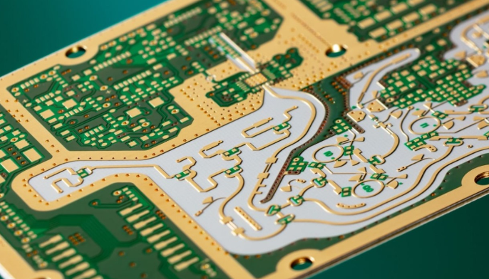
Selective soldering is an advanced soldering technique used in printed circuit board (PCB) assembly to precisely solder specific components without affecting surrounding areas. This process is particularly useful for mixed-technology PCBs containing both surface-mount devices (SMDs) and through-hole components (THCs). This paper explores the principles, methods, equipment, advantages, and challenges of selective soldering, along with its applications in modern electronics manufacturing.
Keywords: Selective soldering, PCB assembly, wave soldering, soldering robots, flux application
1. Introduction
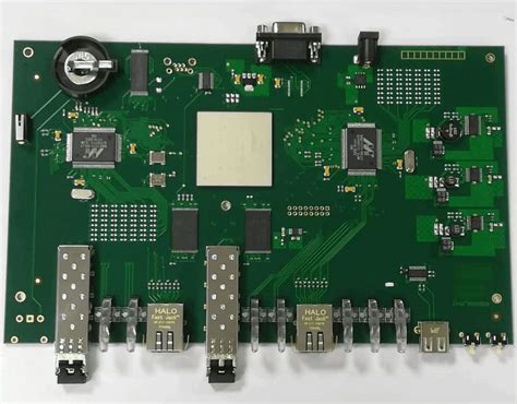
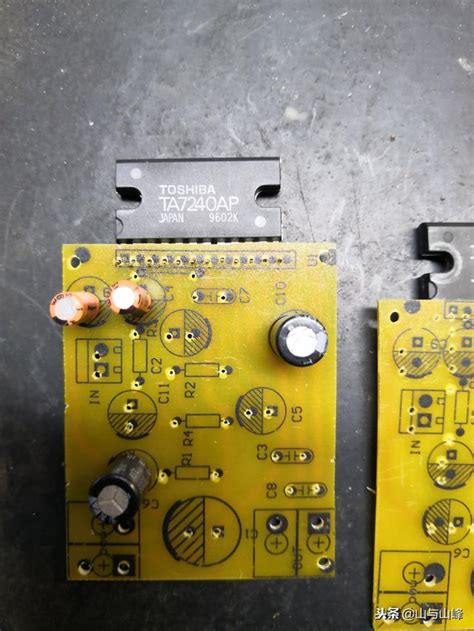
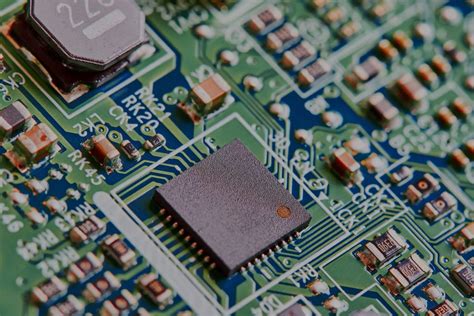
As electronic devices become more complex, PCBs often incorporate a mix of SMDs and THCs. While reflow soldering is ideal for SMDs, THCs traditionally require wave soldering. However, wave soldering exposes the entire PCB to high temperatures, which can damage sensitive components. Selective soldering addresses this issue by targeting only the necessary areas, improving reliability and reducing thermal stress.
2. Selective Soldering Process Overview
Selective soldering involves localized application of solder to specific PCB areas. The key steps include:
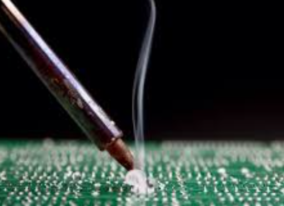
2.1 Flux Application
Flux is applied only to the areas to be soldered, typically via spray, drop jet, or ultrasonic methods. The flux removes oxides and enhances solder wettability.
2.2 Preheating
The PCB is preheated to reduce thermal shock and activate the flux. Preheating methods include infrared (IR) heaters, hot air, or convection.
2.3 Soldering
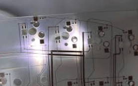
A miniature solder wave or laser soldering is used to melt solder onto the targeted joints. Robotic arms with solder nozzles ensure precision.
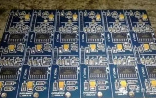
2.4 Cleaning and Inspection
Residual flux is cleaned, and automated optical inspection (AOI) checks for defects like bridging or insufficient solder.

3. Selective Soldering Techniques
3.1 Mini-Wave Selective Soldering
A small solder wave is generated using a nozzle, allowing precise soldering of through-hole components without affecting nearby SMDs.
3.2 Laser Soldering
A focused laser beam heats the solder paste or wire, providing ultra-precise control for high-density PCBs.
3.3 Robotic Soldering
Programmable robotic arms with solder dispensers or wave nozzles adapt to different PCB layouts, ideal for low-to-medium volume production.
4. Advantages of Selective Soldering
- Precision: Only targeted areas are soldered, reducing thermal stress on sensitive components.
- Flexibility: Suitable for mixed-technology PCBs with fine-pitch components.
- Reduced Defects: Minimizes solder bridging and flux residues.
- Cost-Effective for High-Mix Production: Eliminates the need for custom pallets used in wave soldering.
5. Challenges and Solutions
- Process Complexity: Requires precise control of temperature, flux, and solder flow.
- Equipment Cost: Higher initial investment than wave soldering.
- Throughput Limitations: Slower than mass wave soldering but improving with multi-nozzle systems.
6. Applications
- Automotive Electronics: Engine control units (ECUs) with mixed components.
- Aerospace and Defense: High-reliability PCBs requiring minimal thermal stress.
- Medical Devices: Sensitive implantable electronics.
- Industrial IoT: Durable PCBs for harsh environments.
7. Conclusion
Selective soldering is a critical advancement in PCB assembly, enabling high-precision soldering for complex, mixed-technology boards. While it requires sophisticated equipment and process optimization, its benefits in reliability and flexibility make it indispensable in modern electronics manufacturing. Future advancements may include AI-driven adaptive soldering and faster multi-zone systems.