PCB signal traces are hotter than we thought

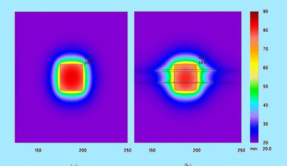
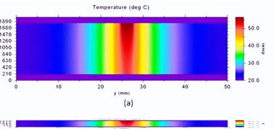
Figure 1(a), shows a simulation of vertical heat flow from a trace across the board to the other side. Simulations are for 100 mil wide, 1.0 oz. On the top layer of a 63 mil thick FR4 board, the thick traces are heated to almost 58 oC. This number seems impressive, but it is misleading in a very important sense. Horizontal and vertical scales are very different. The image represents a cross-sectional area that is only 63 mils (1.6 mm) thick but 2.0 inches (50 mm) wide.
Vertical heat flow through PCB
Figure 1(b) is the same thermal image shown approximately to scale. Looking at it this way, it’s obvious that due to the board’s geometry and thermal thinness, there is very little chance of horizontal heat escaping from the traces. This means that the bottom layer of the board will have (approximately) the same heat distribution as the top layer. This means that all the layers in between will also have the same heat distribution – the current passing through the trace will not only heat the trace, but also everything underneath it.
Heating pad
Recently, we performed an interesting set of simulations (see [2] and [3]) that further explored this relationship. Figure 2 represents a portion of this simulation. We started with a 250 x 125mm FR4 board, 1.6mm thick. The top layer has two 25 x 25 mm copper pads. The copper pad is heated by applying 2.5 watts of power to it. A 125 x 125 mm copper plane is placed on the bottom layer only on the left side of the board.
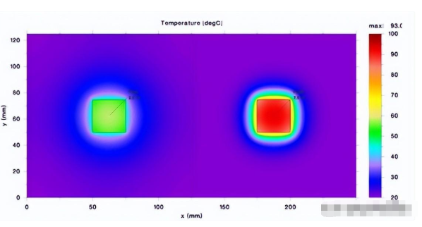
Figure 2. Two pads heated with 2.5 watts. There is a large flat surface under the left pad.
The applied power heats the right pad (without bottom layer) to 93 oC above the ambient temperature of 73 oC. Place a flat surface under the pad (left side of the image) to reduce the pad temperature to 59 oC. But what’s really interesting is what happens under the hood, as shown in Figure 3.
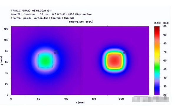
Figure 3. Bottom layer of the circuit board shown in Figure 2.
The heat distribution on the bottom layer (Figure 3) looks very similar to the heat distribution on the top layer (Figure 2). The temperature is almost the same as well. The top temperature of the right heating pad is 93 oC. The temperature in the same area on the bottom floor is about 89 oC, only 4 degrees cooler than the top floor. The temperature of the area under the left pad is about 50 oC, 9 degrees cooler than the top pad.
So, what if we put the plane on the inner layer of the circuit board? Figure 4 shows the thermal distribution of the bottom layer when the plane is placed on the inner layer 0.5 mm below the left pad. The right area under the heating pad is still only 4 degrees cooler than the top pad. The closer plane reduces the temperature of the top left pad to about 45 oC. The corresponding temperature for the bottom layer is about 39 oC, which is 6 degrees cooler than the top layer.
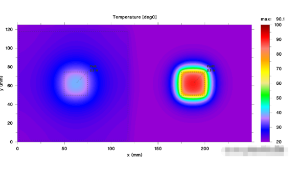
Figure 4. Heat distribution in the bottom layer if the inner plane is placed 0.5 mm below the top layer.
Interestingly, the presence of a copper plane tends to lower overall temperatures because horizontal heat flow is better, but it has a much smaller effect on the overall thermal pattern. Even if there is a copper plane on the bottom layer (Figure 2), the heat distribution on the plane is similar to the heat distribution above it. Significant thermal gradients can (and do exist) across copper surfaces and planes, and this is emphasized in many places in our book [1].
These results illustrate an important fact: the heat distribution on the bottom layer of the board is similar to the heat distribution on the top layer. The point temperature difference between the top and bottom layers is typically less than 10 oC, often in the range of 5 oC or even lower.
GET PCB MANUFACTURING AND ASSEMBLY QUOTE NOW!
Heating traces
Nowadays these pads are larger. What happens if we look at a normal sized (heated) trace? We replaced the pads in the simulation with 4 traces 1, 2, 4, and 6 mm wide (approximately 40, 80, 160, and 240 mils, respectively). Each trace carries enough current to raise its temperature (without an underlying plane) to approximately 70 oC. The simulation plane is placed on the bottom layer of the left half of the board. Figure 5 shows the thermal distribution of the top and bottom layers of the simulation.
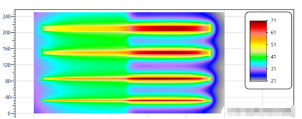
Figure 5. Thermal distribution of the top and bottom layers of the simulated heating trace. In this simulation, there is a flat surface on the bottom layer on the left side of the board. top level
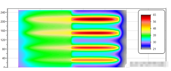
Figure 5. Thermal distribution of the top and bottom layers of simulated heating traces. In this simulation, there is a flat surface on the bottom layer on the left side of the board. Ground floor
We also simulated the board 0.5 mm below the trace on the lower left side of the board (not shown). The results are presented in Table 1. Important results are in the Difference column for each floor configuration (None, Ground Floor, Inner Layer).
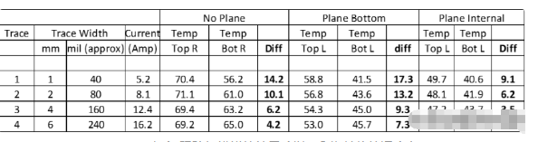
Table 1. Results of trace-level simulations (temperature in oC).
Temperature differences tend to be smallest for the widest traces and increase as the pad/trace width becomes narrower. Still, the local temperature under even the narrowest traces is important. Not discussed here (see again [3]), the temperature difference is a function of board thickness. As the thickness of the circuit board increases, the temperature difference also increases.
The results tend to confirm the general statement above: the heat distribution on the bottom layer of a circuit board is similar to the heat distribution on the top layer. The point temperature difference between the top and bottom layers is typically less than 10 oC, often in the range of 5 oC or even lower.
Related Resources Anritsu adds tools to VNA family to increase signal integrity test capabilities 224 Gb/s per channel: Options and challenges
Influence
The above has several possible meanings. First, these results explain why thermal vias are so inefficient, they are almost ineffective. By definition, thermal vias have to go somewhere. Typically, they terminate on the copper surface (flat surface) on the other side of the board. Equation 1 shows the theory behind them. The heat conduction formula is:
GET PCB AND ASSEMBLY SERVICE QUOTE NOW!
Equation 1. Q/t = kA(ΔT)/d
Where:
Q/t = heat transfer rate (watts or joules/second)
k = thermal conductivity (W/m·K)
ΔT = temperature change (oC = oK)
A = overlapping area
d = distance between pad and plane
In the example above (Figures 2 and 3), the heating pad (without an underlying plane) is 73 oC warmer than the ambient temperature (ΔT=73). But in this case, there is nowhere to terminate the thermal via. When we add a plane on the bottom layer we can terminate the thermal via and the ΔT (between pad and plane) is reduced to 9 oC. (The internal plane case reduces ΔT to 6 oC.) Almost all of the benefit comes from the addition of the copper plane itself. The marginal contribution of the additional thermal vias is almost negligible.
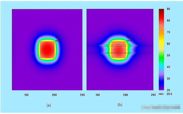
The second implication is that smaller signal traces on inner layers will have nearly the same thermal distribution as the top and bottom layers above and below them. Figure 6(b) illustrates an internal trace layer, approximately 6 mils below the top layer, passing underneath one of our heating pads (with no plane underneath). There are two traces, 1.0 mm and 2.0 mm (40 and 80 mil) wide, that pass under the pad. Figure 6(a) is the same pad without any traces.

Figure 6. Comparison of thermal patterns under a heated pad with no internal traces (a) and with 6 mils of internal traces under the pad (b).
The thermal pattern illustrates that traces have little impact on cooling (the smaller the traces, the smaller the effect), but in general, signal traces have almost the same thermal distribution as heating pads. Since resistivity is a function of temperature, this means that the resistance of a signal trace changes from point to point along the trace as it passes under the pad [4]. Presumably, this means that the resistance on each side of a differential pair, or the resistance of different differential pairs in a signal bus, may be different if they pass through different thermal environments. This may or may not have an impact on signal levels and timing, depending on the situation.
experimental evidence
An appropriate question is: Do we have any experimental evidence to support the type of thermal profiles we discuss here? The answer is yes. For example, in a recent article [5] we (experimentally) showed that traces routed under a pad change resistance if the pad temperature changes. We then asked if this had any signal integrity implications.
In our book [1] we devote Chapter 8 to passing heating. In that chapter, we have two tables to confirm that our simulation model matches our experimental test board [6]. Figures 7 and 8 are adapted from Figures 8.8 and 8.9 in that chapter. These thermal images are from an experimental 6-inch trace with a via in the middle, going from the top layer to the bottom layer. The left portion of each trace is on top. The temperature indication on the left is for the traces/vias on this top layer. The right part of each image is the temperature of the top layer, heated by the actual trajectory of the bottom layer.
In Figure 7, the top layer on the right is approximately 10 degrees lower than the equivalent location on the opposite layer. But in Figure 8, the difference is only about one or two degrees lower than the opposite layer. This is consistent with our simulation above. As the heating width increases, the temperature difference decreases.
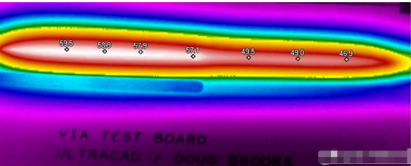
Figure 7. 27 mil wide trace carrying 6.65 amps (Adapted from [1], Figure 8.8.)
Figure 8. 200-mil wide trace carrying 8.55 amps (Adapted from Reference 1, Figure 8.9)
bottom line
The thermal effects of heated traces and pads are not limited to the circuit board layer on which they are located. They are reflected to a greater or lesser extent on every layer above and below them.