PCB Stack-up Design: Layer Count Estimation and Manufacturability Considerations
Abstract
Printed Circuit Board (PCB) stack-up design is a critical aspect of modern electronics development, directly impacting signal integrity, power distribution, thermal management, and ultimately the manufacturability of the final product. This paper examines the methodologies for estimating appropriate PCB layer counts during the initial design phase and analyzes key manufacturability factors that influence stack-up decisions. We explore the relationship between circuit complexity, performance requirements, and physical constraints, providing guidelines for optimizing layer configurations while maintaining production feasibility.
1. Introduction
As electronic devices continue to increase in complexity while shrinking in physical size, PCB stack-up design has become increasingly challenging. The selection of an appropriate layer count and stack-up configuration affects not only the electrical performance but also the cost, reliability, and manufacturability of the PCB. This paper addresses two fundamental aspects of PCB stack-up design: (1) methodologies for estimating the required number of layers early in the design process, and (2) manufacturability considerations that constrain stack-up options.
2. PCB Layer Count Estimation
2.1 Factors Influencing Layer Count Requirements
Several key factors determine the minimum number of layers required for a PCB design:
- Component Density and Pin Count: High-density designs with BGAs or complex ICs typically require more layers for escape routing.
- Signal Integrity Requirements: High-speed signals often need dedicated reference planes and controlled impedance layers.
- Power Distribution Network (PDN) Complexity: Multiple voltage domains may necessitate additional power planes.
- EMI/EMC Considerations: Shielding layers may be required for sensitive circuits.
- Thermal Management: Additional copper layers may be needed for heat dissipation.
2.2 Estimation Methodologies
2.2.1 Pin Density Method
One established approach uses pin density to estimate layer requirements:
Estimated Layers = (Total Pins × Routing Channel Utilization) / (Available Tracks per Layer)Where:
- Total Pins = sum of all component pins
- Routing Channel Utilization = typically 0.5-0.7 for dense designs
- Available Tracks per Layer = (Board Area)^0.5 / (Trace Width + Clearance)
2.2.2 BGA Breakout Analysis
For designs dominated by high-pin-count BGAs, the layer count is often determined by breakout requirements:
- Calculate required escape vias per BGA:
- For perimeter arrays: 4 × (Number of Rows – 1)
- For full arrays: Approximately 60-70% of total balls
- Determine available routing channels between pads
- Calculate layers needed to route all signals
2.2.3 Signal Layer Estimation
High-speed designs may require additional layers based on:
- Number of controlled impedance signals
- Required impedance matching (differential pairs, etc.)
- Crosstalk avoidance requirements
A rough estimate for signal layers:
Signal Layers ≈ (Total High-Speed Nets × Average Length) / (Board Area × Routing Efficiency)2.3 Layer Count Optimization
After initial estimation, designers should:
- Evaluate layer sharing possibilities (mixed signal/power layers)
- Consider via technologies (blind/buried vias can reduce layer count)
- Assess routing completion percentage (aim for 80-90% completion after initial estimation)
3. Manufacturability Considerations
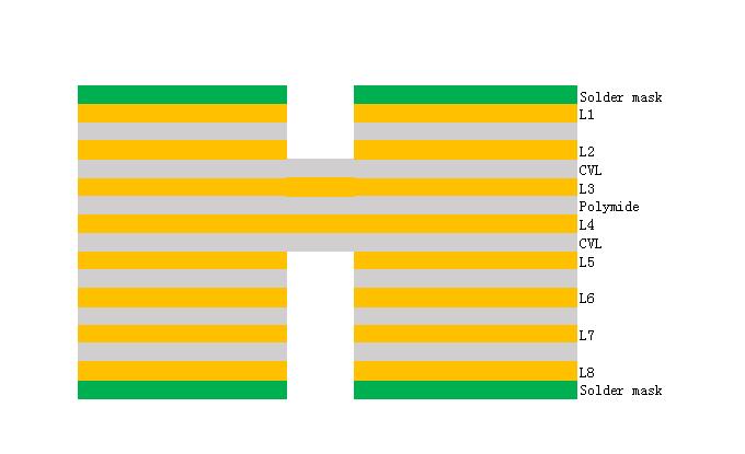
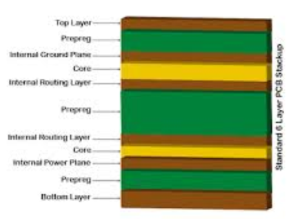
3.1 Standard Stack-up Configurations
Common manufacturable layer configurations include:
- 4-layer: Signal1 – GND – PWR – Signal2
- 6-layer: S1 – GND – S2 – PWR – GND – S3
- 8-layer: S1 – GND – S2 – PWR – GND – S3 – PWR – S4
Deviations from standard configurations may increase cost and reduce yield.
3.2 Material Selection and Thickness
Manufacturability depends on:
- Core/Prepreg Thickness: Standard thicknesses (e.g., 0.2mm, 0.4mm) are preferred
- Copper Weight: 1oz (35μm) is most common; >2oz may require special processing
- Dielectric Constant Consistency: Important for impedance control
3.3 Aspect Ratio Constraints
The drill-to-board thickness ratio affects plating quality:
Maximum Aspect Ratio = 8:1 (standard), up to 10:1 (advanced)This limits minimum via sizes for thick boards.
3.4 Impedance Control
Controlled impedance designs require:
- Precise dielectric thickness control (±10%)
- Consistent copper etching (trace width tolerance ±15%)
- Material with stable Dk values across production panels
3.5 High-Density Interconnect (HDI) Considerations
For HDI designs:
- Sequential lamination cycles increase cost
- Laser-drilled microvias have minimum diameter limits (typically 75-100μm)
- Stacked vs. staggered via configurations affect reliability
3.6 Thermal Management
Manufacturing constraints include:
- Maximum copper area per layer (typically 70-80% for reliable etching)
- Thermal relief requirements for PTH components
- Via-in-pad design rules
3.7 Cost vs. Layer Count Relationship
Approximate cost increase per additional layer:
| Layer Count | Cost Multiplier |
|---|---|
| 2L | 1.0x |
| 4L | 1.8-2.2x |
| 6L | 2.5-3.0x |
| 8L | 3.5-4.5x |
| 10L+ | 5.0x+ |
4. Design for Manufacturing (DFM) Guidelines
To ensure manufacturability:
- Symmetrical Stack-ups: Prevent warpage by balancing copper distribution
- Even Layer Counts: Odd counts may require special processing
- Standard Materials: Use FR-4 unless high-frequency requirements dictate alternatives
- Consistent Spacing: Maintain minimum 3x dielectric thickness between planes
- Via Protection: Tent vias or fill vias in high-stress areas
5. Case Studies
5.1 Consumer IoT Device
- Requirements: 500 pins, 2 BGA packages, 10+ high-speed signals
- Estimated layers: 6 (using pin density method)
- Final stack-up: 6-layer with 2 signal, 2 plane, 2 mixed layers
- Manufacturability: Standard FR-4, 1oz copper, 1.6mm final thickness
5.2 High-Speed Network Processor
- Requirements: 2500 pins, 4 high-pin-count BGAs, 100+ differential pairs
- Estimated layers: 12 (BGA breakout limited)
- Final stack-up: 12-layer HDI with microvias
- Manufacturability: Requires sequential lamination, laser drilling
6. Future Trends
- Embedded Components: May reduce surface routing layers
- Advanced Materials: Enable thinner dielectrics for more layers in same thickness
- Additive Processes: Could enable more complex 3D layer structures
7. Conclusion
Effective PCB stack-up design requires balancing electrical requirements with manufacturing realities. Early layer count estimation using pin density, breakout analysis, and signal integrity requirements helps establish feasible starting points. Designers must then consider material constraints, aspect ratios, impedance control, and cost factors to develop manufacturable stack-ups. As technology advances, the relationship between layer count estimation and manufacturability will continue to evolve, requiring designers to stay informed about new materials and processes.