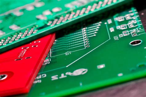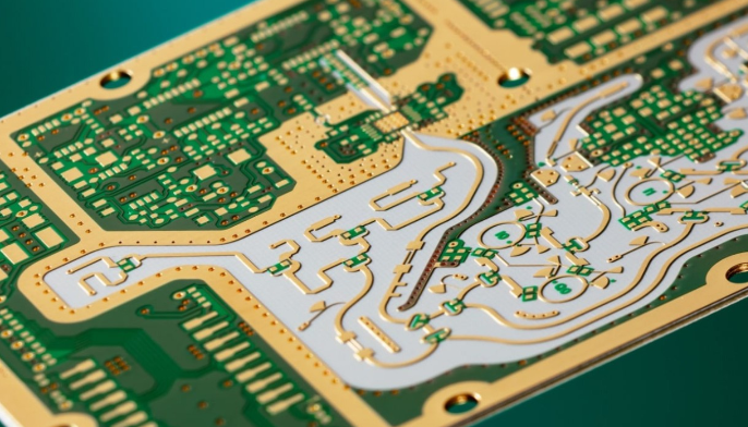
PCB Stackup: Plan, Design, Make and Repeat
PCB stackup design is similar to making burgers. Burger shops prepare each layer of burgers carefully, just like PCB manufacturers stack PCB boards together. Burgers come in different sizes and shapes, with a variety of toppings, and secret sauces covering our own toast. Just like we use different types of metal cores on PCBs, we also offer a variety of patties.
Now you may wonder how we make the best circuit boards in the world.
Let me tell you our secret, it’s all about PCB stackup. Stacking is an important part of the PCB design and manufacturing process. A good stackup design is key to reducing the electromagnetic radiation of electronic circuits.
- Thus improving the overall signal integrity of the circuit board. On the other hand, a poor stackup design can lead to higher electromagnetic radiation and signal loss. Every PCB designer’s job must include reducing the electromagnetic radiation of PCB loops caused by differential mode noise and common mode radiation.
Modern electronics revolves around the miniaturization of electronic components.
Among electronic manufacturers, there is a widely popular trend to pack more processing power into a small package. Strictly speaking, from an electronics perspective, the smaller the form factor, the better.
- Industry experts predict that we will soon reach the physical limits of transistor-level electronic components. Nevertheless, we believe that a PCB designer can work wonders at the design level, making PCBs smaller and denser with the help of expert manufacturers like us.
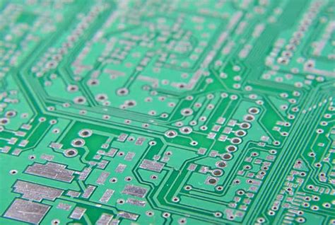
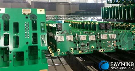
Differences between Standard Stackup and HDI Stackup
Often overlooked, it is very important to understand the differences between HDI stackup and standard stackup. The main reason is the long list of advantages associated with HDI stackup technology, including higher component density per square inch, lower aspect ratio, and fewer layers compared to standard stackup.
Standard stackup design depends on the number of signal layers.
For standard PCB stackup, key parameters include the number of layers, number of ground and power planes, circuit frequency, layer sequence, and power requirements. Some additional parameters include the spacing between layers and shielded or unshielded enclosures.
Key design rules for standard stackup include maintaining space between signal layers and using large cores to avoid EMC issues. It is worth mentioning that the main advantage of standard stackup is the shielding of the inner layers by the planes of the outer layers. However, the main disadvantage includes the reduction of ground planes due to the presence of component mounting pads, especially on high-density PCBs.
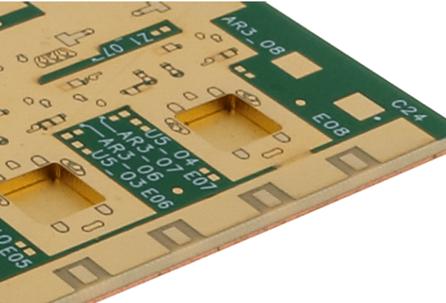
HDI stackup technology is a cutting-edge technology that is revolutionizing the design and manufacturing of multi-layer PCBs.
HDI provides a sequential build for the stackup, thus allowing for more design options. HDI simplifies the design architecture of complex circuit boards. In addition, HDI stackup uses blind and buried vias, as well as stacked and staggered vias. HDI stackup architecture follows a slightly different approach compared to standard stackup. The number of layers is determined by the number of balls. Other factors that affect the stackup include the number of signal layers, power layers, and ground layers.
In addition, it is recommended that the number of planes and signal layers of HDI stackup should be odd or even (even numbers for both are best for a balanced structure). The layers should be placed symmetrically. Microvia structures have a great impact on the manufacturing process as they directly affect the number of lamination cycles, unlike standard stackups. Of course, HDI does not require complex architectures. One of the most common mistakes designers make is to create unnecessarily complex architectures.
Stackup Planning Tools
There are a few HDI stackup planning tools available on the market today. Stackup planning tools will ensure that the HDI printed circuit board design will be manufactured the first time. The tool creates technology level categories to give you a better idea of the level of technology complexity required for different traces and different via sizes. Because high density integrated circuit boards are worth the extra cost, try the free tool: HDI Stackup Planner!
HDI Stackup Architecture Example
- HDI stackup architecture is divided into stackup classes based on the number of board layers and sequential lamination of the HDI board. These levels are determined by the formula X-N-X, where X is the number of laminations required on both sides of the board and N is the number of signal layers. It must be noted that as the requirement for sequential lamination increases, the price of the board will increase.
- Therefore, single layer laminations manufactured with laser drills will be more profitable. This stackup class is a no-brainer in terms of utilizing micro vias in the cheapest way possible. Using laser drills will allow designers to achieve smaller pad and via sizes. This helps alleviate some design constraints and reduce design time.
- The more variations in the layers where the micro vias start and stop, the more sequential lamination is required for PCB manufacturing. Any layer where a micro via starts or stops requires a substructure, and each substructure requires an additional lamination cycle. (Lamination process is defined as the process of pressing a set of copper layers with uncured dielectric between two adjacent copper layers into a multi-layer PCB laminate by applying heat and pressure).
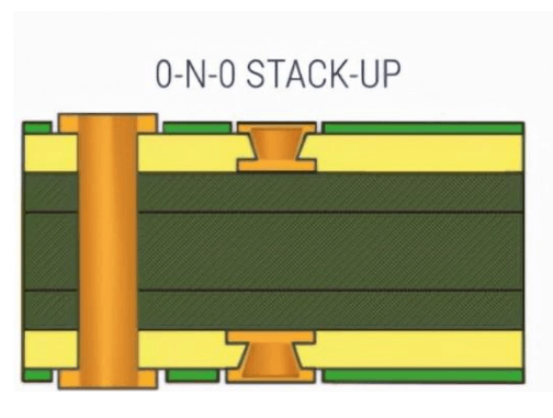
0-N-0 Stackup
The cost and complexity of the board increases with the number of process steps associated with stackup. Additional manufacturing processes also mean more yield loss. N represents the number of layers in the first or base lamination (or core stackup), and 0 means there are no sequential lamination steps and no additional dielectric and copper layers. Below is an example of a 0-N-0 stackup,
1-N-1 Stackup
Sequential laminations 1-1 on either side of the core 1-1. One sequential lamination adds two copper layers for a total of N+2 layers. This stackup design has no stacked vias. There is an additional lamination with no stacked vias. The buried vias are drilled mechanically. There is no need to use conductive filler for the vias. It will naturally fill with dielectric material. The second lamination adds the top and bottom layers. Then, we finish with the last mechanical drill. Here are the steps for 1-N-1 stackup,
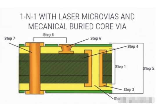
The core is laminated. (The core can only be two layers, so there is no lamination.)
The core is mechanically drilled.
The mechanical drill is plated.
The second layer is imaged/etched.
Two additional layers are added by sequential lamination. (The mechanical drill is now a buried via.)
Laser drilled holes are formed.
The final vias are formed.
Laser drilled holes and vias are plated.
The PCB manufacturer plans to add the right amount of prepreg between layer 1 and layer 2 so that the resin flows into the buried vias.
How to achieve the best PCB stackup design
Whether it is HDI or standard stackup board, following certain guidelines, according to the application and its requirements is the best possible way to achieve PCB stackup design. We have listed some guidelines to help you achieve the possible PCB stackup design,
A) The number of signal layers is important
PCB stackup depends on the number of signal layers present in the design. Signal layers vary with the application of the PCB. For example, high-speed signals or high-power applications may require more layers than low-speed signal levels.
Complex devices with low pitch and high pin counts, such as BGAs, often require more signal layers. Signal integrity requirements, such as very low crosstalk, may also lead to an increase in the number of signal layers.
Mixed signal types – a large number of analog and digital signals will require separation between these two types and may increase the number of signal layers.
B) Number of ground and power planes:
The use of ground and power planes allows designers to allocate signal layers purely for signal routing; they also reduce the DC resistance in the power and ground rails, thereby ensuring less DC voltage drop across the device.
A ground plane is a copper plane in the PCB that is connected to the power ground connection. A power plane is a copper plane in the PCB that is connected to the power rails.
These planes also provide a signal return path for time-varying and high-frequency signals and help significantly reduce noise and signal crosstalk, thereby improving signal integrity. Power planes also improve the capacitive decoupling capabilities of the PCB circuit. Planes also improve electromagnetic compatibility performance by reducing electromagnetic radiation.
C) Controlled Impedance Routing
Controlled impedance is the characteristic impedance of a transmission line formed by a PCB trace and its associated reference plane. It is relevant when high frequency signals propagate on a PCB transmission line. Uniform controlled impedance is important to achieve good signal integrity, i.e. the propagation of the signal without significant distortion.
Also read our article Specifying Controlled Impedance Requirements .
- When the reference plane is not the next layer down, there is a chance that another copper feature on the next layer will become the reference.
- From a manufacturing perspective, we need to maintain uniform etching across the length of the line, both in width and trapezoidal. This is why etch tolerance and uniformity come into play.
D) Sequential Layer Arrangement
Another critical aspect of stack design is sequential layer arrangement. Arranging high speed signal layers according to the thickness of the microstrip line is one of the key parameters that designers must consider before routing. Placing the signal layer below the power plane will allow for tight coupling.
For accurate layer placement, a minimum distance is maintained between the power and ground planes. Other key parameters include avoiding placing two signal layers next to each other, and establishing a symmetrical stack of the top and bottom layers.
In sequential lamination, try to limit the number of lamination steps as it becomes more expensive and time consuming.
E) Determine Layer Material Types
An important consideration for PCB stackup is the thickness of each signal layer. This should be determined along with determining the thickness of the prepreg and core material. There are standard thicknesses and other properties for different board material types. Your selection process for PCB materials should include these electrical, mechanical, and thermal properties.
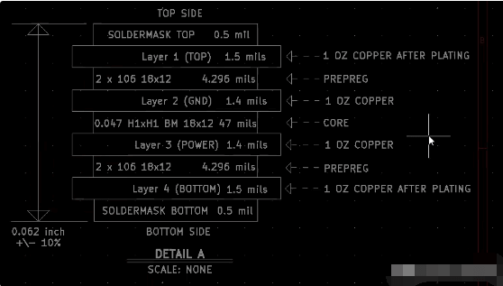
Stackup Example 10-layer stackup with ground plane for each signal layer
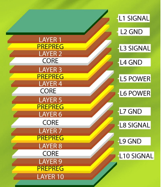
Typical 10-layer stackup with ground plane for each signal layer
10-layer stackup
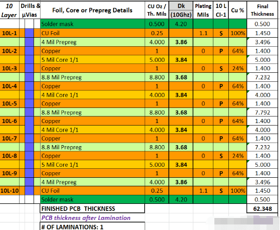
Another 10-layer stackup example
12-layer stackup
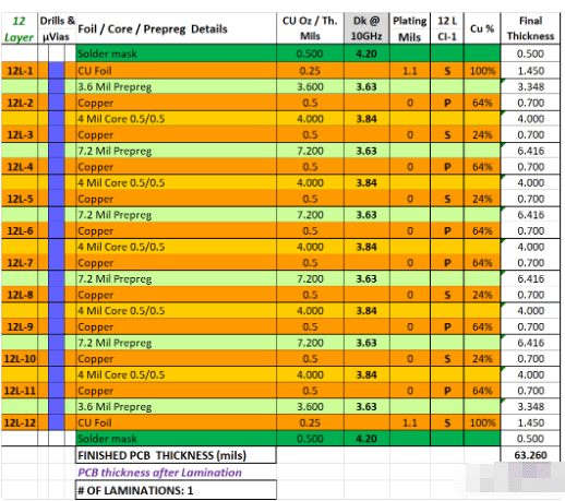
An example of a 12-layer PCB stackup
PCB stackup in e-CAD tool
Screenshot of PCB stackup in e-CAD tool