Pcb test
Importance Of PCB Testing In Electronics Manufacturing
In the realm of electronics manufacturing, the significance of Printed Circuit Board (PCB) testing cannot be overstated. As the backbone of virtually all electronic devices, PCBs serve as the foundation upon which electronic components are mounted and interconnected. Consequently, ensuring their reliability and functionality is paramount to the success of any electronic product. PCB testing, therefore, plays a crucial role in the manufacturing process, safeguarding against potential failures and ensuring that the final product meets the highest standards of quality and performance.
To begin with, PCB testing is essential for identifying defects that may arise during the manufacturing process.
These defects can range from simple issues such as incorrect component placement to more complex problems like short circuits or open circuits. By employing a variety of testing methods, manufacturers can detect these issues early in the production cycle, thereby reducing the risk of costly recalls or product failures in the field. This proactive approach not only enhances the reliability of the product but also helps maintain the manufacturer’s reputation for quality.
Moreover, PCB testing is instrumental in verifying the functionality of the board.
This involves ensuring that the board performs its intended functions under various conditions. Functional testing, for instance, simulates the operational environment of the PCB to confirm that it behaves as expected. This step is critical in identifying any discrepancies between the design specifications and the actual performance of the board. By addressing these discrepancies before the product reaches the market, manufacturers can avoid potential malfunctions that could lead to customer dissatisfaction or even safety hazards.
In addition to defect detection and functionality verification, PCB testing also contributes to the optimization of the manufacturing process.
By analyzing test data, manufacturers can identify patterns or trends that may indicate underlying issues in the production line. This information can then be used to refine manufacturing techniques, improve yield rates, and reduce waste. Consequently, PCB testing not only ensures product quality but also enhances overall production efficiency, leading to cost savings and increased competitiveness in the market.
Furthermore, the importance of PCB testing extends to compliance with industry standards and regulations.
In many sectors, electronic products must adhere to stringent safety and performance standards. PCB testing provides the necessary documentation and evidence to demonstrate compliance with these requirements. This is particularly important in industries such as automotive, aerospace, and medical devices, where the failure of an electronic component can have severe consequences. By ensuring that their products meet all relevant standards, manufacturers can avoid legal liabilities and gain the trust of their customers.
In conclusion, PCB testing is a vital component of the electronics manufacturing process. It serves multiple purposes, from detecting defects and verifying functionality to optimizing production and ensuring compliance with industry standards. By investing in comprehensive PCB testing, manufacturers can enhance the quality and reliability of their products, reduce costs, and maintain a competitive edge in the market. As technology continues to evolve and the demand for high-performance electronic devices grows, the role of PCB testing in ensuring product excellence will only become more critical.
Common Methods For PCB Testing And Their Applications
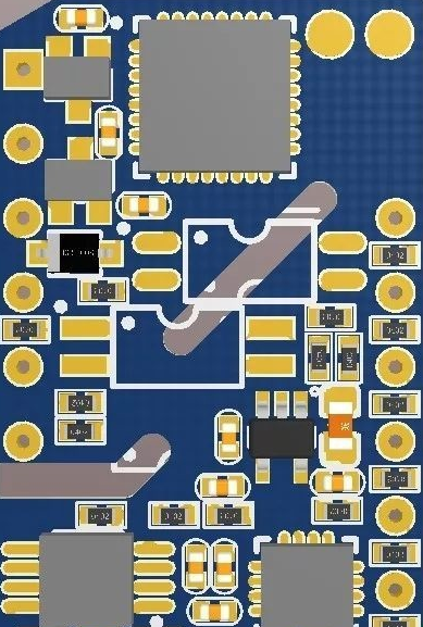
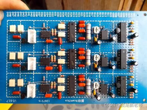
Printed Circuit Boards (PCBs) are integral components in modern electronic devices, serving as the backbone for electrical connectivity and functionality. Ensuring their reliability and performance is crucial, which necessitates rigorous testing methods. Various techniques are employed to assess the quality and functionality of PCBs, each with its specific applications and advantages. Understanding these methods is essential for manufacturers and engineers aiming to produce high-quality electronic products.
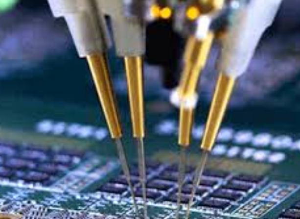
One of the most prevalent methods for PCB testing is the In-Circuit Test (ICT).
This technique involves using a bed of nails fixture to make contact with various test points on the PCB. ICT is highly effective for detecting manufacturing defects such as shorts, opens, and incorrect component values. It is particularly useful in high-volume production environments due to its speed and accuracy. However, the initial setup cost can be high, making it less suitable for low-volume or prototype testing.
Transitioning to another widely used method, Functional Testing (FT) evaluates the overall performance of the PCB by simulating its operational environment.
This method ensures that the board functions as intended when integrated into the final product. Functional testing is versatile and can be customized to test specific functionalities of the PCB. It is often used in conjunction with ICT to provide a comprehensive assessment of the board’s quality. While functional testing is invaluable for verifying performance, it may not pinpoint the exact location of a defect, which can be a limitation in troubleshooting.
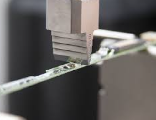
Another critical method is Automated Optical Inspection (AOI), which uses cameras to visually inspect PCBs for defects such as soldering issues, component misalignment, and surface defects.
AOI is non-contact and can be performed at various stages of the manufacturing process, making it a flexible option for quality control. Its ability to quickly identify visual defects makes it an essential tool in ensuring the aesthetic and functional integrity of PCBs. However, AOI is limited to detecting only visible defects and cannot assess electrical performance.
Complementing AOI, Automated X-ray Inspection (AXI) provides a deeper level of analysis by examining the internal structures of the PCB.
AXI is particularly useful for inspecting solder joints in complex assemblies, such as those involving Ball Grid Arrays (BGAs), where visual inspection is insufficient. This method can detect hidden defects that are not visible to the naked eye, offering a significant advantage in quality assurance. Despite its benefits, AXI is more expensive and time-consuming than AOI, which may limit its use to critical applications.
Flying Probe Testing (FPT) offers an alternative to ICT for low-volume production and prototype testing.
This method uses moving probes to contact test points on the PCB, eliminating the need for a custom fixture. FPT is highly flexible and can be quickly adapted to different board designs, making it ideal for testing small batches or new designs. However, it is generally slower than ICT, which can be a drawback in high-volume production scenarios.
In conclusion, the choice of PCB testing method depends on various factors, including production volume, cost considerations, and the specific requirements of the application. By employing a combination of these testing techniques, manufacturers can ensure the reliability and performance of their PCBs, ultimately leading to the production of high-quality electronic devices. Understanding the strengths and limitations of each method allows for informed decision-making and optimization of the testing process.
Innovations In Automated PCB Testing Technologies
In recent years, the field of printed circuit board (PCB) testing has witnessed significant advancements, driven by the increasing complexity and miniaturization of electronic components. As the demand for more efficient and reliable electronic devices grows, so does the need for innovative testing technologies that can ensure the quality and functionality of PCBs. Automated PCB testing technologies have emerged as a critical component in the manufacturing process, offering enhanced precision, speed, and cost-effectiveness.
One of the most notable innovations in automated PCB testing is the development of advanced optical inspection systems.
These systems utilize high-resolution cameras and sophisticated image processing algorithms to detect defects on the surface of PCBs. By capturing detailed images of the board, optical inspection systems can identify issues such as misaligned components, soldering defects, and surface contamination. This non-contact method of inspection not only reduces the risk of damage to delicate components but also allows for rapid assessment, significantly increasing throughput in manufacturing environments.
In addition to optical inspection, automated X-ray inspection has become an indispensable tool in PCB testing.
X-ray systems provide a non-destructive means of examining the internal structure of PCBs, making it possible to detect hidden defects such as voids in solder joints, internal cracks, and misaligned layers. The ability to visualize the internal composition of a PCB without disassembly is particularly valuable for complex multilayer boards, where traditional inspection methods may fall short. As X-ray technology continues to evolve, improvements in resolution and speed are further enhancing its applicability in high-volume production settings.
Moreover, the integration of artificial intelligence (AI) and machine learning into PCB testing processes is revolutionizing the way defects are identified and analyzed.
AI algorithms can be trained to recognize patterns and anomalies in test data, enabling more accurate and efficient defect detection. By continuously learning from new data, these systems can adapt to changes in manufacturing processes and component designs, ensuring that testing remains effective even as technology evolves. The use of AI in automated testing not only reduces the likelihood of human error but also allows for predictive maintenance, where potential issues can be identified and addressed before they lead to costly failures.
Another significant advancement in automated PCB testing is the implementation of in-circuit testing (ICT) systems.
ICT involves the use of a bed-of-nails fixture to make electrical contact with various points on a PCB, allowing for comprehensive testing of individual components and circuits. This method is particularly effective for detecting functional defects and verifying the performance of complex boards. Recent innovations in ICT technology have focused on improving the accuracy and speed of testing, as well as reducing the physical footprint of test equipment, making it more suitable for modern manufacturing environments.
Furthermore, the advent of wireless testing technologies is opening new possibilities for PCB testing.
Wireless systems eliminate the need for physical connections between the test equipment and the PCB, reducing setup time and minimizing the risk of damage to the board. These systems are particularly advantageous for testing flexible and rigid-flex PCBs, where traditional contact-based methods may be challenging to implement.
In conclusion, the landscape of automated PCB testing technologies is rapidly evolving, driven by the need for more efficient, accurate, and cost-effective solutions. Innovations such as advanced optical and X-ray inspection, AI integration, in-circuit testing, and wireless testing are transforming the way PCBs are evaluated, ensuring that electronic devices meet the highest standards of quality and reliability. As these technologies continue to advance, they will play an increasingly vital role in supporting the ever-growing demands of the electronics industry.
Challenges And Solutions In PCB Test Design
Printed Circuit Board (PCB) testing is a critical phase in the electronics manufacturing process, ensuring that the final product functions as intended. However, designing effective PCB tests presents several challenges that require innovative solutions. Understanding these challenges and their corresponding solutions is essential for engineers and manufacturers striving to maintain high-quality standards and reduce time-to-market.
One of the primary challenges in PCB test design is the increasing complexity of modern electronic devices.
As devices become more sophisticated, PCBs must accommodate a higher density of components and intricate circuit layouts. This complexity makes it difficult to access test points and increases the likelihood of defects. To address this, engineers are turning to advanced testing methodologies such as boundary scan testing and automated optical inspection (AOI). Boundary scan testing allows for the examination of interconnections on PCBs without physical probes, while AOI uses cameras to visually inspect boards for defects, thus overcoming the limitations of traditional testing methods.
Another significant challenge is the miniaturization of components.
As consumer demand for smaller, more portable devices grows, components on PCBs are becoming increasingly compact. This miniaturization complicates the testing process, as traditional test equipment may not be able to accurately assess these tiny components. To mitigate this issue, manufacturers are investing in high-precision testing equipment capable of handling smaller components. Additionally, non-contact testing methods, such as X-ray inspection, are gaining popularity as they can effectively evaluate the integrity of solder joints and other critical areas without physical contact.
The rapid pace of technological advancement also poses a challenge for PCB test design.
As new technologies emerge, testing methodologies must evolve to keep pace. This requires continuous investment in research and development to create innovative testing solutions that can accommodate new materials, components, and design techniques. Collaboration between manufacturers, testing equipment providers, and research institutions is crucial in developing these cutting-edge solutions. By working together, these stakeholders can ensure that testing methodologies remain relevant and effective in the face of technological change.
Cost is another factor that cannot be overlooked in PCB test design.
Developing and implementing comprehensive testing procedures can be expensive, particularly for small and medium-sized enterprises. To address this, companies are increasingly adopting a risk-based approach to testing, focusing resources on the most critical areas of the PCB that are likely to impact performance. This targeted approach helps to optimize testing budgets while still ensuring product quality. Additionally, the use of simulation software can reduce costs by allowing engineers to identify potential issues in the design phase, before physical prototypes are produced.
Finally, the need for rapid time-to-market adds pressure to the PCB testing process.
In a competitive market, delays in testing can lead to missed opportunities and lost revenue. To expedite the testing process, manufacturers are leveraging automation and data analytics. Automated testing systems can perform repetitive tasks more quickly and accurately than human operators, while data analytics can provide insights into test results, helping engineers to identify patterns and potential issues more efficiently.
In conclusion, while PCB test design presents numerous challenges, there are a variety of solutions available to address these issues. By embracing advanced testing methodologies, investing in high-precision equipment, fostering collaboration, adopting risk-based approaches, and leveraging automation and data analytics, manufacturers can overcome these challenges and ensure the production of high-quality electronic devices. As technology continues to evolve, so too must the strategies and tools used in PCB testing, ensuring that they remain effective and relevant in an ever-changing landscape.