Pcb v-score guidelines
Understanding PCB V-Score Guidelines: A Comprehensive Overview
Printed Circuit Boards (PCBs) are integral components in modern electronic devices, and their design and manufacturing processes are critical to the functionality and reliability of the final product.
One of the essential techniques in PCB manufacturing is V-scoring, a method used to facilitate the separation of individual boards from a larger panel.
Understanding PCB V-score guidelines is crucial for engineers and manufacturers to ensure precision, efficiency, and quality in the production process.
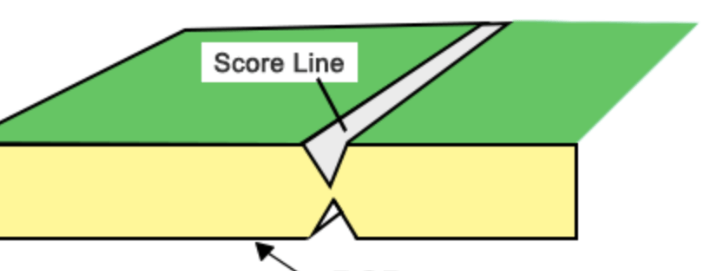
V-scoring involves creating a V-shaped groove on both sides of the PCB, which allows for easy breaking or snapping of the board along the scored line.
This technique is particularly useful in high-volume production, where multiple PCBs are fabricated on a single panel and need to be separated quickly and cleanly. The depth and angle of the V-score are critical parameters that must be carefully controlled to achieve the desired results.
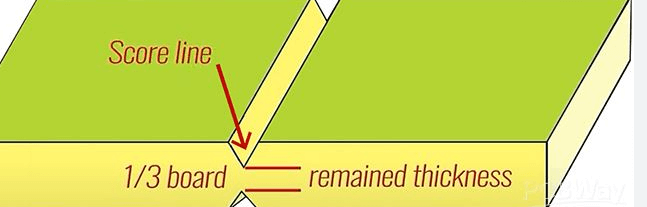
To begin with, the depth of the V-score is typically specified as a percentage of the total board thickness.
Common practice dictates that the score depth should be between 30% to 40% of the board’s thickness on each side. This ensures that the remaining material is sufficient to hold the boards together during handling and assembly but weak enough to allow for easy separation. For instance, if a PCB has a thickness of 1.6mm, the V-score depth would be approximately 0.5mm to 0.6mm on each side.
Moreover, the angle of the V-score is another critical factor.
The standard angle for V-scoring is 30 degrees, which provides a balance between ease of separation and structural integrity. A sharper angle might make the board too fragile, while a wider angle could make it difficult to break the boards apart cleanly. Therefore, adhering to the standard 30-degree angle is generally recommended unless specific design requirements dictate otherwise.
In addition to depth and angle, the spacing between V-scores is an important consideration.
The minimum spacing is typically determined by the width of the cutting tool and the mechanical properties of the PCB material. Ensuring adequate spacing helps prevent damage to the boards during the scoring process and subsequent separation. It is also essential to consider the placement of components and traces near the V-score lines. Components should be positioned at a safe distance from the score lines to avoid damage during separation, and traces should be routed to minimize the risk of electrical shorts or breaks.
Furthermore, it is important to note that V-scoring is not suitable for all PCB designs.
For instance, boards with complex shapes or those requiring high mechanical strength may not be ideal candidates for V-scoring. In such cases, alternative methods like routing or tab-routing with perforations might be more appropriate. Therefore, careful evaluation of the design requirements and manufacturing constraints is necessary to determine the most suitable separation technique.
In conclusion, understanding PCB V-score guidelines is essential for achieving optimal results in PCB manufacturing. By carefully controlling the depth and angle of the V-score, ensuring adequate spacing, and considering the placement of components and traces, manufacturers can produce high-quality PCBs that meet the desired specifications. While V-scoring offers significant advantages in terms of efficiency and ease of separation, it is crucial to evaluate each design’s unique requirements to select the most appropriate method. Through meticulous planning and adherence to established guidelines, engineers and manufacturers can ensure the reliability and performance of their electronic products.
Best Practices for Implementing PCB V-Score in Design
When designing printed circuit boards (PCBs), implementing V-score techniques can significantly enhance the efficiency and precision of the manufacturing process. V-scoring, a method used to pre-cut PCBs, allows for easier separation of individual boards from a larger panel. To ensure optimal results, it is essential to adhere to best practices that encompass both design and manufacturing considerations.
First and foremost, understanding the fundamental principles of V-scoring is crucial.
V-scoring involves creating a V-shaped groove on both sides of the PCB, which weakens the material along a predetermined line. This groove typically penetrates 30-40% of the board’s thickness, allowing for easy snapping apart of the individual boards after assembly. The depth and angle of the V-score must be carefully calculated to maintain the structural integrity of the PCB while ensuring ease of separation.
One of the primary considerations in V-score implementation is the layout of the PCB.
Designers should strategically place V-scores to avoid critical components and traces. It is advisable to maintain a safe distance, typically around 1mm, between the V-score line and any nearby components or copper traces. This precaution helps prevent damage during the separation process and ensures the functionality of the final product.
Moreover, the orientation of the V-score lines should be aligned with the natural break lines of the PCB.
This alignment minimizes stress on the board and reduces the risk of damage. Additionally, designers should consider the direction of the V-score relative to the grain of the PCB material. Aligning the V-score with the grain can enhance the ease of separation and improve the overall quality of the final product.
Another critical aspect is the selection of appropriate V-score parameters.
The depth and angle of the V-score must be tailored to the specific requirements of the PCB. For instance, thicker boards may require deeper V-scores to ensure effective separation, while thinner boards may necessitate shallower grooves to maintain structural integrity. Collaborating with the PCB manufacturer during the design phase can provide valuable insights into the optimal V-score parameters for a given project.
Furthermore, it is essential to consider the impact of V-scoring on the assembly process.
The separation of individual boards should be smooth and precise to avoid any damage to the components or solder joints. To achieve this, designers can incorporate breakaway tabs or mouse bites along the V-score lines. These features provide additional support during the separation process and help maintain the alignment of the boards.
In addition to design considerations, proper communication with the PCB manufacturer is vital. Providing detailed documentation, including the exact location and specifications of the V-scores, ensures that the manufacturer can accurately implement the design. Clear communication helps avoid any misunderstandings and ensures that the final product meets the desired quality standards.
Lastly, it is important to conduct thorough testing and inspection of the V-scored PCBs.
This step helps identify any potential issues or weaknesses in the design and allows for necessary adjustments before mass production. By rigorously testing the separation process, designers can ensure that the final product meets the required performance and reliability standards.
In conclusion, implementing PCB V-score techniques requires careful consideration of various design and manufacturing factors. By adhering to best practices, such as strategic placement of V-scores, appropriate parameter selection, and effective communication with the manufacturer, designers can optimize the efficiency and quality of the PCB manufacturing process. Through meticulous planning and testing, the successful implementation of V-scoring can significantly enhance the overall performance and reliability of the final product.
Common Mistakes to Avoid in PCB V-Score Implementation
Implementing V-scoring in printed circuit board (PCB) design is a critical process that requires precision and attention to detail. However, several common mistakes can compromise the integrity and functionality of the final product. Understanding these pitfalls is essential for engineers and designers to ensure optimal performance and manufacturability.
One prevalent mistake in PCB V-score implementation is the improper selection of V-score depth.
The depth of the V-score cut is crucial as it determines the ease of separating individual boards from the panel. If the score is too deep, it can weaken the structural integrity of the PCB, leading to potential breakage during handling or assembly. Conversely, if the score is too shallow, it can make depaneling difficult, increasing the risk of damaging the board or its components. Therefore, it is imperative to adhere to manufacturer guidelines and industry standards when determining the appropriate V-score depth.
Another common error is neglecting the impact of V-scoring on component placement.
Components placed too close to the V-score line can be damaged during the depaneling process. This is particularly true for surface-mounted devices (SMDs) and other delicate components. To avoid this, designers should maintain a safe distance between the V-score line and any critical components. This distance can vary depending on the board’s thickness and the components’ sensitivity, but a general rule of thumb is to keep components at least 1mm away from the V-score line.
In addition to component placement, the orientation of the V-score lines is another factor that can lead to issues if not properly considered.
V-score lines should be aligned with the grain of the PCB material to minimize stress and potential warping. Misalignment can cause the board to bend or twist, which can affect the performance and reliability of the final product. Ensuring that V-score lines are correctly oriented with respect to the PCB’s grain direction is a simple yet effective way to prevent such problems.
Furthermore, inadequate communication with the PCB manufacturer is a mistake that can lead to significant issues.
Designers must provide clear and detailed specifications for V-scoring, including the desired depth, width, and spacing of the score lines. Failure to do so can result in misinterpretations and errors during the manufacturing process. Establishing a robust line of communication with the manufacturer and providing comprehensive design files can help mitigate these risks.
Another aspect that is often overlooked is the consideration of the PCB’s overall design and layout.
V-scoring should be integrated into the design process from the beginning, rather than being an afterthought. This holistic approach ensures that all aspects of the PCB, including component placement, routing, and mechanical constraints, are taken into account. By incorporating V-scoring into the initial design phase, designers can avoid many of the common pitfalls associated with its implementation.
Lastly, it is essential to conduct thorough testing and validation of the V-scored PCBs.
This includes both visual inspections and functional testing to ensure that the boards can be easily and safely separated without compromising their integrity. Regular testing and quality control measures can help identify and address any issues early in the production process, thereby reducing the risk of defects and improving overall product quality.
In conclusion, avoiding common mistakes in PCB V-score implementation requires careful consideration of various factors, including V-score depth, component placement, line orientation, communication with manufacturers, and overall design integration. By paying attention to these details and adhering to best practices, designers can ensure the successful implementation of V-scoring in their PCB projects, leading to reliable and high-quality products.
Comparing PCB V-Score with Other Depaneling Methods
When it comes to the manufacturing of printed circuit boards (PCBs), the depaneling process is a critical step that ensures individual boards are separated from a larger panel without causing damage. Among the various methods available, PCB V-scoring stands out for its unique advantages and specific applications. However, to fully appreciate its benefits, it is essential to compare it with other depaneling methods such as routing, laser cutting, and punching.
PCB V-scoring involves making V-shaped grooves on both sides of the PCB, allowing the boards to be easily snapped apart.
This method is particularly advantageous for high-volume production runs due to its cost-effectiveness and speed. The V-scoring process is relatively simple and requires minimal setup time, making it an attractive option for manufacturers looking to optimize production efficiency. Additionally, V-scoring minimizes material waste, as the grooves are typically very narrow, thus preserving more of the PCB material for use.
In contrast, routing, another common depaneling method, involves using a mechanical router to cut out individual boards from the panel.
While routing offers high precision and can handle complex board shapes, it is generally slower and more expensive than V-scoring. The mechanical nature of routing also generates more dust and debris, which can be problematic in cleanroom environments. Furthermore, the wider kerf of the router bit results in more material waste compared to the narrow grooves of V-scoring.
Laser cutting is another alternative that offers high precision and the ability to cut intricate designs.
This method uses a focused laser beam to separate the boards, providing a clean and burr-free edge. However, laser cutting equipment is significantly more expensive than the machinery required for V-scoring. Additionally, the process can be slower, especially for thicker boards, and may require more maintenance due to the wear and tear on the laser optics.
Punching, a method often used for high-volume production, involves using a die to stamp out individual boards from the panel.
This method is extremely fast and can handle large quantities efficiently. However, the initial cost of creating custom dies can be prohibitive, especially for smaller production runs or designs that frequently change. Punching also lacks the precision of routing or laser cutting, making it less suitable for boards with intricate designs or tight tolerances.
When comparing these methods, it becomes clear that each has its own set of advantages and limitations.
V-scoring is particularly well-suited for straightforward, high-volume production runs where cost and speed are primary considerations. Its simplicity and efficiency make it a preferred choice for many manufacturers. However, for applications requiring high precision or intricate designs, routing or laser cutting may be more appropriate despite their higher costs and slower speeds. Punching, while extremely fast, is best reserved for very high-volume runs where the cost of custom dies can be justified.
In conclusion, the choice of depaneling method depends largely on the specific requirements of the production run, including factors such as volume, design complexity, and budget. PCB V-scoring offers a balanced approach, providing a cost-effective and efficient solution for many applications. By understanding the strengths and limitations of each method, manufacturers can make informed decisions that optimize their production processes and meet their specific needs.


