PCB vs. PCBA: Understanding the Key Differences
Introduction
In the electronics manufacturing industry, two terms that are often used interchangeably but have fundamentally different meanings are PCB and PCBA. While both are essential components of modern electronic devices, they represent distinct stages in the electronics production process. This article will explore the key differences between Printed Circuit Boards (PCBs) and Printed Circuit Board Assemblies (PCBAs), examining their definitions, manufacturing processes, components, applications, and testing requirements. Understanding these differences is crucial for engineers, procurement specialists, and anyone involved in electronics design and manufacturing.
Definition and Basic Concepts
What is a PCB?
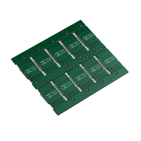
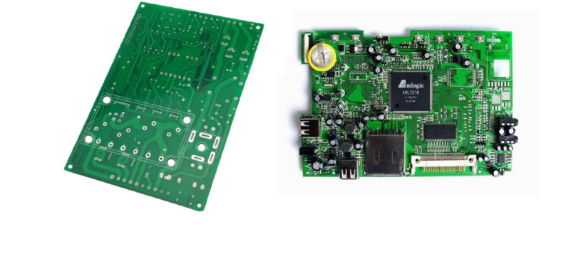
A Printed Circuit Board (PCB) is the foundational physical platform that mechanically supports and electrically connects electronic components using conductive tracks, pads, and other features etched from copper sheets laminated onto a non-conductive substrate. PCBs can be single-sided (one copper layer), double-sided (two copper layers), or multi-layer (outer and inner layers of copper).
The bare PCB serves as the base structure before any components are attached. It consists of several key elements:
- Substrate material (typically FR-4 fiberglass)
- Copper traces that form the electrical connections
- Solder mask that protects the copper from oxidation and prevents solder bridges
- Silkscreen for component labels and identifiers
What is a PCBA?
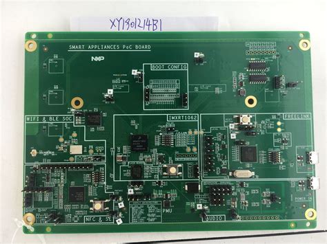
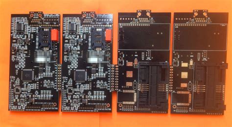
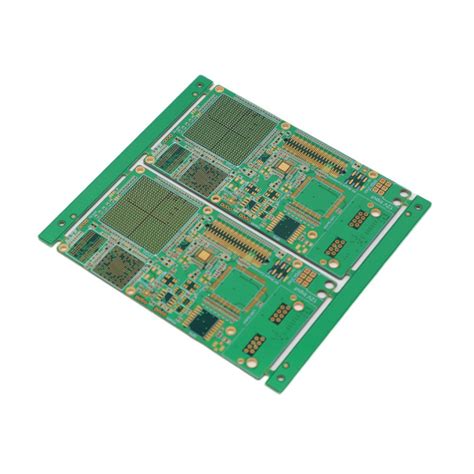
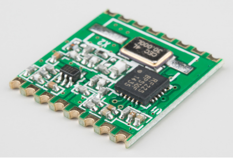
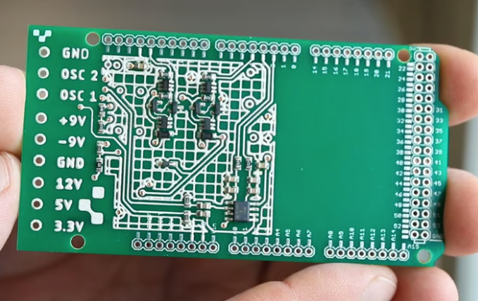
A Printed Circuit Board Assembly (PCBA) refers to a PCB that has completed the assembly process and has all the necessary electronic components soldered onto it. The PCBA is essentially a “populated” PCB that is ready for installation in an electronic device or for further testing.
The transition from PCB to PCBA involves:
- Placement of electronic components (resistors, capacitors, ICs, etc.)
- Soldering components to the board (through-hole or surface mount)
- Potential conformal coating or other protective treatments
- Functional testing to verify proper assembly
Manufacturing Process Differences
PCB Fabrication Process
The creation of a bare PCB involves multiple specialized steps:
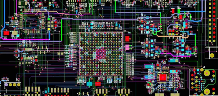
- Design and Layout: Using ECAD software to create the circuit schematic and board layout
- Printing the Design: Transferring the design to the board material
- Etching: Removing unwanted copper to leave only the desired traces
- Drilling: Creating holes for through-hole components and vias
- Plating: Adding copper to hole walls for electrical connectivity
- Solder Mask Application: Applying the protective layer
- Silkscreen Printing: Adding labels and identifiers
- Surface Finish: Applying finishes like HASL, ENIG, or OSP
- Testing: Electrical testing for continuity and isolation
- Routing: Cutting the panel into individual boards
This process focuses solely on creating the physical board without any components attached.
PCBA Manufacturing Process
The PCBA process builds upon the completed PCB through these key steps:
- Solder Paste Application: Applying solder paste to pads (for SMT components)
- Component Placement: Precisely placing components using pick-and-place machines
- Reflow Soldering: Melting solder paste to create permanent connections
- Through-Hole Component Insertion: For traditional components (if applicable)
- Wave Soldering: For through-hole components (alternative to hand soldering)
- Inspection: Automated optical inspection (AOI) and manual checks
- Testing: Functional testing of the assembled board
- Conformal Coating: Applying protective layers (if required)
- Final Assembly: Adding connectors or other mechanical components
The PCBA process transforms the bare PCB into a functional electronic assembly.
Component Considerations
PCB Components
A bare PCB contains no active or passive electronic components. The only “components” are the physical structures that make up the board itself:
- Conductive copper traces and planes
- Dielectric substrate material
- Solder mask material
- Silkscreen markings
- Vias and through-holes
- Edge connectors and contact fingers
- Mechanical features (mounting holes, cutouts)
These elements are all passive and serve to provide the foundation for component attachment rather than performing any electronic function.
PCBA Components
A PCBA includes all the active and passive components that give the board its electronic functionality. These can include:
Surface Mount Devices (SMD):
- Resistors, capacitors, inductors
- Integrated circuits (ICs)
- Transistors and diodes
- LEDs and other optoelectronic components
- Connectors and sockets
Through-Hole Components:
- Larger capacitors and resistors
- Transformers and coils
- Some connectors and switches
- Heat sinks and mechanical supports
Other Possible Additions:
- Batteries and power supplies
- Displays and touchscreens
- Sensors and actuators
- Shielding cans or EMI protection
Functional Differences
PCB Functionality
A bare PCB by itself has no electronic functionality. Its purposes are:
- Physical Support: Provides a rigid (or flexible) structure to mount components
- Electrical Connectivity: Offers pre-designed pathways for electrical signals
- Thermal Management: Includes features for heat dissipation (in some designs)
- Mechanical Interface: Provides mounting points and connections to other systems
Without components, a PCB cannot process signals, amplify power, or perform any of the functions expected of an electronic device.
PCBA Functionality
A PCBA represents a complete electronic circuit capable of performing its intended functions:
- Signal Processing: Can receive, process, and output electronic signals
- Power Management: Can regulate, convert, and distribute power
- Data Processing: For digital boards, can perform computations
- Interface Capability: Can communicate with other devices and users
- System Control: Can execute programmed operations and responses
The PCBA is what transforms the potential of the PCB design into actual electronic functionality.
Testing and Quality Control
PCB Testing
Testing for bare PCBs focuses on the integrity of the board itself:
- Continuity Testing: Verifies all desired connections are present
- Isolation Testing: Ensures no unintended connections exist
- Impedance Testing: For high-speed designs, verifies characteristic impedance
- Visual Inspection: Checks for physical defects and manufacturing flaws
- Dimensional Verification: Ensures the board meets specified measurements
These tests verify that the PCB matches the design specifications before components are added.
PCBA Testing
PCBA testing is more complex and evaluates both the assembly quality and functional performance:
- Automated Optical Inspection (AOI): Checks component placement and solder joints
- In-Circuit Testing (ICT): Tests individual components and connections
- Functional Testing: Verifies the assembled board performs as intended
- Boundary Scan Testing: For digital circuits, tests IC interconnections
- Burn-in Testing: Stresses the assembly to identify early failures
- Environmental Testing: Evaluates performance under various conditions
PCBA testing must verify not only that components are properly attached but that the complete assembly functions correctly.
Cost Structure Differences
PCB Costs
The cost of a bare PCB is determined by:
- Board Size: Larger boards use more material
- Layer Count: More layers increase complexity and cost
- Materials: Special substrates (high-frequency, flexible) cost more
- Tolerances: Tighter design rules increase manufacturing difficulty
- Quantity: Economies of scale reduce per-unit costs
- Surface Finish: Different finishes have varying costs
- Lead Time: Faster turnaround typically costs more
PCBA Costs
PCBA costs include the PCB plus additional factors:
- Component Costs: Varies greatly depending on BOM complexity
- Assembly Complexity: Higher component density increases cost
- Labor Costs: Manual assembly steps add expense
- Testing Requirements: More comprehensive testing increases cost
- Yield Losses: Defective assemblies affect overall cost
- Packaging: Special packaging requirements may add cost
- Certifications: Industry-specific certifications can increase costs
Generally, the PCBA cost is significantly higher than the bare PCB cost due to the added components and assembly processes.
Design Considerations
PCB Design Focus
When designing a PCB, engineers concentrate on:
- Signal Integrity: Proper trace routing and impedance control
- Power Distribution: Adequate power and ground planes
- Thermal Management: Heat dissipation considerations
- Manufacturability: Design for fabrication constraints
- Mechanical Fit: Physical dimensions and mounting requirements
- Testability: Access points for testing bare boards
PCBA Design Focus
PCBA design expands on PCB design with additional considerations:
- Component Placement: Optimal positioning for performance and manufacturability
- Soldering Requirements: Adequate spacing and pad design
- Test Access: Points for functional testing
- Rework Potential: Design for possible repair and rework
- Environmental Protection: Needs for conformal coating or encapsulation
- Supply Chain: Component availability and sourcing
Applications and Use Cases
PCB Applications
Bare PCBs are typically handled by:
- PCB Manufacturers: Who produce the boards
- Assembly Houses: Who turn them into PCBAs
- Hobbyists and Engineers: Who may manually assemble prototypes
- Research Facilities: For experimental designs
- Educational Institutions: For teaching purposes
PCBA Applications
Completed PCBAs are found in virtually all electronic devices:
- Consumer Electronics: Smartphones, TVs, computers
- Industrial Equipment: Control systems, automation
- Medical Devices: Diagnostic equipment, implants
- Automotive Systems: Engine controls, infotainment
- Aerospace and Defense: Avionics, communication systems
- IoT Devices: Sensors, smart home products
Industry Standards and Certifications
PCB Standards
Relevant standards for PCBs include:
- IPC-6011: Generic Performance Specification for PCBs
- IPC-6012: Qualification and Performance Specification for Rigid PCBs
- IPC-A-600: Acceptability of Printed Boards
- UL 94: Flammability Rating for PCB Materials
- IPC-2221: Generic Standard on Printed Board Design
PCBA Standards
Additional standards apply to PCBAs:
- IPC-A-610: Acceptability of Electronic Assemblies
- IPC-J-STD-001: Requirements for Soldered Electrical and Electronic Assemblies
- ISO 9001: Quality Management Systems
- IEC 61191: Requirements for Printed Board Assemblies
- IPC-7351: Generic Requirements for Surface Mount Design
Environmental and Reliability Factors
PCB Environmental Considerations
For bare PCBs:
- Material Selection: Choosing appropriate substrates for the operating environment
- Surface Finish: Selecting finishes that resist corrosion
- Thermal Properties: Ensuring the board can withstand processing temperatures
- Storage Conditions: Proper storage to prevent oxidation or moisture absorption
PCBA Environmental Considerations
For assembled PCBAs:
- Component Ratings: Ensuring all parts meet environmental requirements
- Conformal Coating: Protection against moisture, chemicals, and contaminants
- Thermal Management: Adequate heat dissipation for all components
- Mechanical Stress: Vibration and shock resistance
- Operating Conditions: Temperature, humidity, and pressure ranges
Future Trends and Developments
PCB Innovations
Emerging trends in PCB technology:
- High-Density Interconnect (HDI): Finer traces and spaces
- Flexible and Rigid-Flex PCBs: For wearable and compact devices
- Embedded Components: Passive components within the board layers
- Advanced Materials: High-frequency and thermal-conductive substrates
- 3D Printed Electronics: Additive manufacturing of circuits
PCBA Innovations
Advancements in PCBA technology:
- Advanced Packaging: Chip-scale packaging, 3D IC stacking
- Automated Optical Inspection: AI-enhanced defect detection
- Robotic Assembly: More flexible and precise component placement
- Environmentally Friendly Processes: Lead-free and low-VOC materials
- Smart Manufacturing: IoT-enabled assembly lines for real-time monitoring
Conclusion
While PCB and PCBA are related terms in electronics manufacturing, they represent fundamentally different stages of product development. A PCB is the bare, unpopulated board that provides the physical foundation and electrical connections, while a PCBA is the complete, functional assembly with all components installed. Understanding these differences is essential for effective communication in the electronics industry, accurate project planning, and proper expectations regarding capabilities, costs, and testing requirements.
The transformation from PCB to PCBA represents the crucial step between design and functionality in electronic devices. As technology advances, both PCBs and PCBAs continue to evolve, with innovations in materials, manufacturing processes, and design approaches pushing the boundaries of what’s possible in electronics. Whether you’re an engineer, procurement specialist, or electronics enthusiast, recognizing the distinction between these two critical elements of electronic devices will serve you well in all aspects of electronics design, manufacturing, and application.