PCB Wiring Rules: A Comprehensive Guide
Introduction to PCB Wiring
Printed Circuit Board (PCB) wiring is the fundamental process of creating electrical connections between components on a PCB. Proper wiring is essential for ensuring signal integrity, minimizing electromagnetic interference (EMI), and maintaining overall circuit reliability. As electronic devices become more complex and operate at higher frequencies, adherence to proper wiring rules becomes increasingly critical.
PCB wiring involves more than simply connecting points A to B; it requires careful consideration of current capacity, signal timing, thermal management, and manufacturability. This article explores the essential rules and best practices for effective PCB wiring, covering everything from basic principles to advanced techniques for high-speed designs.
Fundamental PCB Wiring Rules
1. Trace Width Considerations
The width of PCB traces directly affects their current-carrying capacity and resistance. Key considerations include:
- Current Capacity: Wider traces can handle more current without overheating. Use online calculators or IPC-2152 standards to determine appropriate widths for your current requirements.
- Voltage Drop: Narrow traces have higher resistance, which can cause significant voltage drops in high-current paths.
- Manufacturing Limits: Typical minimum trace widths are 5-6 mils (0.127-0.152 mm) for standard PCBs, though advanced manufacturers can go smaller.
2. Clearance and Creepage
Maintaining proper spacing between conductors is crucial for safety and functionality:
- Electrical Clearance: The shortest air distance between two conductors to prevent arcing. This depends on voltage levels and environmental conditions.
- Creepage Distance: The shortest path along the surface of the insulation material between conductors. Important for high-voltage applications where surface contamination could create leakage paths.
3. Routing Angles
Proper routing angles affect signal integrity and manufacturability:
- Avoid Acute Angles: Use 45° angles or curved traces instead of 90° angles to prevent acid traps during etching and impedance discontinuities.
- Smooth Transitions: Gradual changes in direction help maintain consistent impedance and reduce reflections.
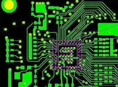
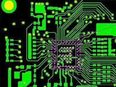
4. Via Usage
Vias connect different layers of the PCB but introduce their own challenges:
- Size Selection: Balance between current capacity (larger vias) and board space (smaller vias).
- Placement: Avoid placing vias in high-current paths or sensitive analog areas when possible.
- Thermal Relief: Use thermal relief patterns for vias connected to ground/power planes to aid soldering.
Signal Integrity Considerations
1. Impedance Control
Maintaining consistent impedance is critical for high-speed signals:
- Microstrip/Stripline: Understand the difference between surface traces (microstrip) and embedded traces (stripline) and their impedance characteristics.
- Calculations: Use field solvers or online calculators to determine required trace widths for target impedance.
- Reference Planes: Ensure uninterrupted reference planes beneath controlled impedance traces.
2. Length Matching
For differential pairs and parallel buses, trace length matching is essential:
- Tolerance: Typically ±5-10 mils for high-speed signals like DDR memory interfaces.
- Serpentining: Use carefully designed meanders to match lengths without introducing new signal integrity issues.
3. Crosstalk Prevention
Minimize unwanted coupling between signals:
- 3W Rule: Space parallel traces at least three times the trace width apart to reduce crosstalk.
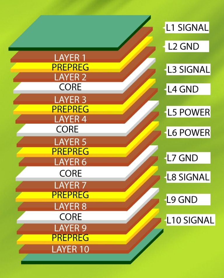
- Layer Stacking: Route adjacent layers orthogonally (horizontal on one layer, vertical on the next) to minimize coupling.
- Guard Traces: Use grounded guard traces between sensitive signals when space permits.
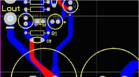
Power Distribution Rules
1. Power Plane Design
Proper power distribution is crucial for stable operation:
- Decoupling: Place decoupling capacitors close to IC power pins with short, wide traces.
- Split Planes: Carefully manage split planes to avoid creating unintended antennas or impedance discontinuities.
- Current Density: Ensure power planes can handle the required current without excessive voltage drop.
2. Star Routing
For sensitive analog circuits or multiple power domains:
- Central Connection: Route power from a central point to different sections to prevent ground loops.
- Separate Returns: Maintain separate return paths for digital and analog sections until they meet at a single point.
EMI/EMC Considerations
1. Return Path Management
Current always returns to its source, and managing this path reduces EMI:
- Continuous Planes: Provide uninterrupted return paths beneath signal traces.
- Split Avoidance: Avoid splitting planes beneath high-speed signal routes.
- Via Stitching: Use multiple vias to connect ground planes at high frequencies.
2. Edge Rate Control
Fast signal edges generate more EMI:
- Series Resistors: Add small series resistors at driver outputs to slow edge rates when possible.
- Filtering: Use appropriate filtering on clock and high-speed signals near board connectors.
Manufacturing Considerations
1. Design for Manufacturability (DFM)
Ensure your design can be reliably produced:
- Annular Rings: Maintain sufficient copper around holes for reliable plating.
- Solder Mask: Define clear solder mask areas to prevent bridging while allowing proper solder flow.
- Silkscreen: Keep reference designators and markings clear but away from pads.
2. Testability
Design with testing and debugging in mind:
- Test Points: Include accessible test points for critical signals.
- Probe Access: Ensure adequate space for oscilloscope or logic analyzer probes.
- Boundary Scan: Consider JTAG/test access for complex digital designs.
Advanced Techniques
1. High-Speed Design Rules
For frequencies above 100MHz or fast edge rates:
- Differential Pairs: Maintain consistent spacing and length matching for differential signals.
- Via Optimization: Use back-drilling or microvias for critical high-speed paths.
- Material Selection: Choose PCB materials with appropriate dielectric constants for your frequency range.
2. RF Considerations
For radio frequency circuits:
- Transmission Lines: Treat all traces as transmission lines with proper termination.
- Component Placement: Minimize path lengths between RF components.
- Shielding: Implement proper shielding techniques for sensitive areas.
Conclusion
PCB wiring is both an art and a science, requiring balance between electrical requirements, physical constraints, and manufacturing realities. By following these wiring rules and understanding the principles behind them, designers can create reliable, high-performance PCBs that meet their design goals while remaining manufacturable.
As technology advances, new challenges emerge in PCB design, but the fundamental principles of proper wiring remain constant. Continuous learning and adaptation to new materials, higher frequencies, and more compact designs will ensure successful PCB implementations in an ever-evolving electronics landscape.
Remember that while rules provide essential guidance, every design presents unique challenges that may require thoughtful deviation from standard practices. The most successful PCB designers combine rigorous adherence to fundamental principles with creative problem-solving to achieve optimal results.