PCBA Essentials: A Guide to Modern Electronics Assembly
Key Takeaways
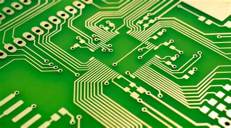
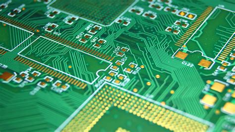
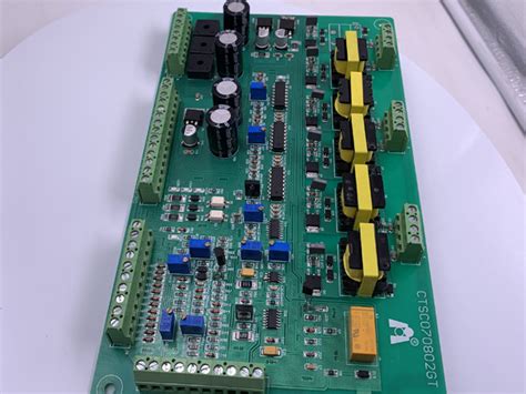
Effective PCBA (Printed Circuit Board Assembly) relies on understanding core principles that bridge design, manufacturing, and functionality. At its foundation, PCB assembly integrates critical components like resistors, capacitors, and integrated circuits onto a printed circuit board, forming the backbone of modern electronics. A well-executed PCBA process balances design precision with manufacturing efficiency, ensuring reliability across applications from consumer gadgets to industrial systems.
Key considerations include selecting high-quality substrates, optimizing component placement for thermal management, and adhering to industry standards (e.g., IPC-A-610). Additionally, advancements in surface-mount technology (SMT) and automated optical inspection (AOI) have streamlined assembly workflows, reducing errors and costs. Challenges such as component miniaturization and supply chain delays demand proactive planning, while robust quality control protocols—including functional testing and X-ray inspection—ensure compliance with performance benchmarks.
By prioritizing design for manufacturability (DFM) and leveraging emerging trends like flexible PCBs and IoT integration, manufacturers can enhance both the cost-effectiveness and scalability of PCBA solutions. These insights lay the groundwork for exploring deeper aspects of electronics assembly in subsequent sections.
Understanding PCBA in Electronics Manufacturing
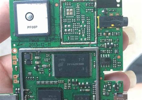
Modern electronics rely on PCBA (Printed Circuit Board Assembly) as the backbone of functional device creation. Unlike standalone PCB (Printed Circuit Board) fabrication, pcb assembly involves mounting and soldering electronic components onto the board, transforming it into an operational system. This process bridges design and functionality, ensuring components like resistors, capacitors, and integrated circuits interact seamlessly.
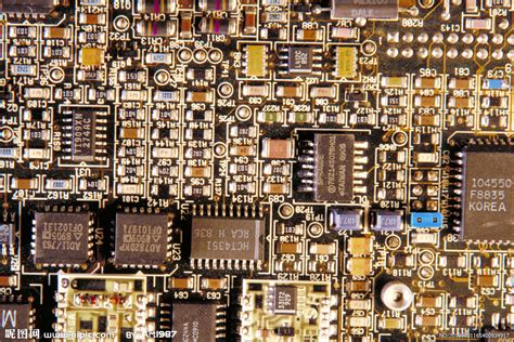
The pcba workflow typically integrates two primary techniques: surface-mount technology (SMT) and through-hole technology (THT). SMT dominates modern assembly due to its efficiency in placing miniature components, while THT remains relevant for high-power or mechanically robust applications.
| Aspect | PCB | PCBA |
|---|---|---|
| Design Focus | Layout & circuitry | Component placement & integration |
| Manufacturing | Etching & drilling | Soldering & testing |
| Application | Bare board | Functional electronic device |
Automation plays a pivotal role in pcb assembly, with pick-and-place machines achieving precision rates exceeding 99.9%. However, human oversight remains critical for quality assurance, particularly in prototyping or low-volume production. As demand for compact, high-performance electronics grows, optimizing pcba processes becomes essential to balance cost, reliability, and innovation.

Key Components of PCBA Design
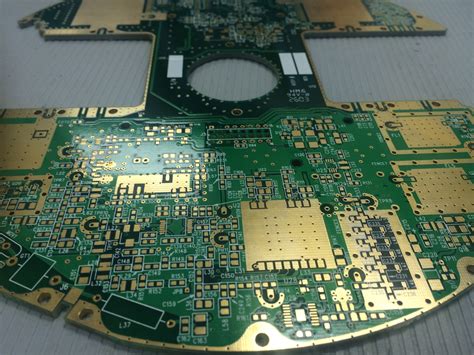
Effective PCBA (Printed Circuit Board Assembly) design hinges on integrating critical elements that ensure functionality, reliability, and manufacturability. At its core, the PCB assembly process relies on three foundational components: the printed circuit board (PCB) substrate, electronic components, and interconnects. The PCB substrate—typically made of FR-4 or high-frequency laminates—serves as the structural base, dictating thermal stability and signal integrity. Component selection, including surface-mount devices (SMDs) and through-hole components, must align with the design’s electrical requirements and assembly feasibility.
Interconnects, such as vias and traces, form the conductive pathways that enable signal transmission and power distribution. Optimizing their layout minimizes electromagnetic interference (EMI) and voltage drops. Additionally, thermal management elements—like heat sinks or thermal pads—are vital for dissipating heat in high-power applications. Designers must also account for test points and debugging interfaces to streamline quality assurance during PCBA production.
A cohesive design integrates design for manufacturability (DFM) principles, balancing component placement density with assembly tolerances. Advanced PCB assembly workflows increasingly leverage automated optical inspection (AOI)-compatible layouts to reduce defects. By harmonizing these elements, engineers create PCBA designs that meet performance benchmarks while aligning with modern electronics assembly standards.
Step-by-Step PCBA Assembly Process
The PCBA process begins with solder paste application, where a stencil ensures precise deposition of solder paste onto designated PCB pads. This step is critical for establishing reliable electrical connections during subsequent stages. Alignment accuracy directly impacts solder joint quality, making automated optical inspection (AOI) systems vital for detecting anomalies.
Next, component placement utilizes high-speed pick-and-place machines to position surface-mount devices (SMDs) and through-hole components. Modern systems achieve placement speeds exceeding 25,000 components per hour while maintaining micron-level precision. Following this, reflow soldering melts the solder paste in a controlled thermal profile, forming permanent electrical bonds.
Tip: Maintain consistent oven temperature zones to prevent defects like tombstoning or cold joints. Post-soldering, AOI and X-ray inspection verify solder integrity, especially for hidden joints in ball-grid arrays (BGAs).
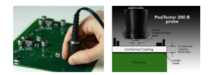
Functional testing then evaluates the assembled PCBA against design specifications, using techniques like in-circuit testing (ICT) or boundary-scan methods. Final conformal coating protects against environmental stressors, completing the PCB assembly cycle. For mixed-technology boards, manual insertion of bulky components may precede or follow automated stages, requiring careful workflow planning.
Throughout the process, traceability systems track components from sourcing to final assembly, ensuring compliance with industry standards like IPC-A-610. By integrating these steps, manufacturers balance speed, precision, and reliability in PCBA production.
Design Considerations for Efficient PCBA
Effective PCBA design requires balancing technical precision with manufacturability. A well-optimized layout begins with strategic component placement, minimizing trace lengths to reduce signal interference and power loss. Thermal management is critical—ensuring adequate spacing between heat-generating components and integrating thermal relief pads prevents overheating during PCB assembly.
Designers must also prioritize signal integrity by adhering to impedance control guidelines and avoiding sharp angles in high-frequency traces. Incorporating Design for Manufacturing (DFM) principles, such as standardized component sizes and panelization strategies, streamlines the PCBA process while reducing material waste.
Material selection plays a pivotal role—choosing substrates with appropriate dielectric properties and copper weights ensures reliability under operational stress. Additionally, test point placement for in-circuit testing (ICT) or automated optical inspection (AOI) simplifies quality checks post-assembly.
Finally, collaboration between design and PCB assembly teams early in the process mitigates errors, ensuring designs align with production capabilities. By addressing these factors, engineers can achieve PCBA solutions that are both cost-effective and performance-driven, laying the groundwork for scalable electronics manufacturing.
Common Challenges in PCB Assembly
While PCB assembly forms the backbone of modern electronics manufacturing, the process often encounters technical and operational hurdles. One prevalent issue stems from component misalignment, particularly with miniaturized parts like 0201 resistors or micro-BGA packages, where even micron-level deviations can compromise functionality. Thermal management during soldering also poses risks—excessive heat may cause warping or delamination, while insufficient temperatures lead to cold joints.
Another critical challenge lies in maintaining PCBA reliability across environmental stressors. Moisture sensitivity in components requires strict handling protocols, as exposure to humidity can trigger popcorn effects during reflow. Signal integrity issues, especially in high-density interconnects (HDI), demand meticulous impedance control to prevent crosstalk or electromagnetic interference (EMI).
Supply chain inconsistencies further complicate PCB assembly, with counterfeit components or delayed material deliveries disrupting production timelines. Additionally, design-for-manufacturability (DFM) oversights—such as inadequate solder mask clearance or improper pad spacing—often surface only during assembly, necessitating costly revisions. Addressing these challenges requires collaboration between design engineers and PCBA specialists to balance performance goals with manufacturable solutions.
PCBA Quality Control Best Practices
Effective PCBA quality assurance begins with rigorous inspection protocols at every production stage. Modern PCB assembly lines integrate automated optical inspection (AOI) systems to detect soldering defects, component misalignment, and trace integrity issues with micron-level precision. For high-density boards, X-ray inspection becomes critical to validate hidden joints and ball grid array (BGA) connections.
A proactive approach involves implementing statistical process control (SPC) to monitor variables like solder paste volume and reflow oven temperature profiles. Adherence to IPC-A-610 standards ensures consistency in acceptability criteria, while first article inspection (FAI) verifies design-to-production alignment. Environmental controls, such as humidity-regulated storage for moisture-sensitive components, prevent oxidation and delamination risks.
Advanced PCBA manufacturers leverage traceability systems with barcoding or RFID tagging to track components from procurement to final testing. Functional testing, including in-circuit testing (ICT) and boundary scan, validates electrical performance against design specifications. For mission-critical applications, environmental stress screening (ESS) simulates operational extremes to identify latent failures.
Collaboration between design and manufacturing teams remains vital—design for manufacturability (DFM) reviews preemptively address potential quality bottlenecks. Regular audits of supplier certifications (e.g., ISO 9001, IATF 16949) and material certifications (e.g., UL, RoHS) further fortify quality frameworks. By embedding these practices, PCB assembly processes achieve near-zero defect rates, ensuring reliability in today’s complex electronic ecosystems.
Future Trends in Electronics Assembly
The evolution of PCBA (Printed Circuit Board Assembly) continues to accelerate as emerging technologies reshape manufacturing paradigms. One key trend is the integration of AI-driven automation in PCB assembly lines, enabling real-time defect detection and predictive maintenance. Advanced machine learning algorithms now optimize component placement accuracy, reducing errors by up to 40% in high-density designs. Another transformative shift is the adoption of additive manufacturing for flexible and hybrid circuits, allowing rapid prototyping of complex PCBA layouts without traditional etching limitations.
Sustainability is also becoming a cornerstone of modern electronics assembly. Manufacturers are prioritizing lead-free soldering techniques and recyclable substrates to meet stringent environmental regulations. Additionally, the rise of IoT-enabled devices demands PCB assembly processes that support miniaturization while maintaining signal integrity—driving innovations in embedded component technology and ultra-thin conductive materials.
As 5G and edge computing proliferate, PCBA designs are evolving to handle higher frequencies and thermal loads, necessitating advanced materials like liquid crystal polymers. Collaborative robotics, paired with digital twin simulations, further streamline workflows, ensuring scalability for mass customization. These trends underscore a future where agility, precision, and eco-consciousness define the next generation of PCB assembly solutions.
Optimizing PCBA for Cost and Performance
Achieving optimal balance between cost efficiency and performance reliability in PCBA requires strategic planning across design, material selection, and manufacturing workflows. Engineers often prioritize component standardization to reduce procurement complexity while maintaining compatibility with automated PCB assembly systems. For instance, selecting surface-mount devices (SMDs) over through-hole components can lower labor costs and improve placement accuracy. However, high-frequency or high-power applications may demand specialized materials like low-loss substrates or thermally conductive laminates, which influence both performance and budget.
Design-for-manufacturing (DFM) principles play a critical role in minimizing rework. This includes optimizing trace widths for current loads, ensuring adequate clearance between components, and avoiding overly complex layouts that strain assembly precision. Advanced simulation tools help identify potential signal integrity or thermal management issues early, reducing post-production fixes.
For cost-sensitive projects, dual sourcing components or leveraging economies of scale in bulk PCBA orders can yield savings without compromising quality. Conversely, mission-critical applications might justify higher-grade materials or redundant circuitry to enhance durability. Rigorous testing protocols—such as automated optical inspection (AOI) and in-circuit testing (ICT)—ensure defects are caught early, aligning long-term reliability with upfront investments. By harmonizing these factors, manufacturers can deliver PCB assembly solutions that meet both technical specifications and financial constraints.
Conclusion
The evolution of PCBA (Printed Circuit Board Assembly) underscores its pivotal role in modern electronics manufacturing. By integrating PCB assembly processes with advanced design principles, manufacturers achieve higher reliability, faster production cycles, and cost-effective scalability. As the electronics industry continues to demand miniaturization and enhanced functionality, optimizing PCBA workflows—from component selection to final testing—remains critical.
Key challenges such as thermal management, signal integrity, and material compatibility require meticulous attention during both design and assembly phases. Adhering to PCB assembly best practices, including rigorous quality control protocols and design-for-manufacturability (DFM) guidelines, ensures robust end products. Looking ahead, emerging trends like automated optical inspection (AOI) and sustainable manufacturing materials will further redefine PCBA standards.
Ultimately, the success of electronic devices hinges on harmonizing innovative PCBA techniques with evolving market needs. Engineers and manufacturers must prioritize continuous learning and adaptation to maintain competitiveness in this dynamic field.
Frequently Asked Questions
What distinguishes PCB assembly from PCBA?
PCB assembly refers to the process of populating a bare PCB (Printed Circuit Board) with electronic components. PCBA (Printed Circuit Board Assembly) denotes the completed board after all components are soldered and tested. Essentially, PCBA represents the functional end product of the PCB assembly process.
How does design impact PCBA reliability?
Poor PCB design—such as improper trace spacing or inadequate thermal management—can lead to signal interference, overheating, or component failure. Following design for manufacturability (DFM) guidelines ensures compatibility with automated PCB assembly equipment, reducing defects and enhancing long-term performance.
What are common challenges in PCB assembly?
Issues like component misalignment, solder bridging, or thermal stress often arise during high-volume production. Advanced techniques like automated optical inspection (AOI) and X-ray testing help identify flaws early, minimizing rework costs and delays.
How is quality controlled in PCBA manufacturing?
Strict quality control protocols include in-circuit testing (ICT), functional testing, and environmental stress screening. These steps validate electrical performance, durability, and compliance with industry standards like IPC-A-610.
What trends are shaping PCBA technology?
Innovations like high-density interconnects (HDI), flexible PCBs, and IoT-driven miniaturization are pushing the boundaries of electronics assembly. Sustainability practices, such as lead-free soldering, are also gaining prominence.
Ready to Optimize Your Next PCBA Project?
For expert guidance on PCB assembly and tailored manufacturing solutions, please click here to explore Andwin PCB’s services.