PCBA Production: Essential Techniques and Modern Applications
Key Takeaways
Effective PCBA (Printed Circuit Board Assembly) production relies on mastering design precision, material selection, and assembly automation. Modern techniques such as Surface Mount Technology (SMT) and Automated Optical Inspection (AOI) ensure high-quality outcomes while minimizing human error.
Tip: Prioritize Design for Manufacturability (DFM) principles early in the pcb assembly process to avoid costly revisions and delays.
Critical considerations include optimizing thermal management and signal integrity to prevent component failure in high-performance applications. Advanced pcba workflows now integrate AI-driven analytics for real-time defect detection, boosting yield rates by up to 30%.
Emerging trends highlight the role of miniaturization and flexible substrates in IoT and wearable devices, where compact pcb assembly designs enable smarter, lighter products. Meanwhile, automotive electronics demand robust pcba solutions capable of withstanding extreme temperatures and vibrations.
Quality control remains non-negotiable, with X-ray inspection and functional testing ensuring compliance with industry standards like IPC-A-610. By adopting these strategies, manufacturers can balance efficiency, reliability, and scalability across diverse applications—from consumer gadgets to industrial systems.
PCBA Production Techniques Overview
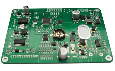
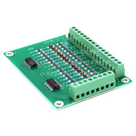
Modern PCBA (Printed Circuit Board Assembly) manufacturing combines precision engineering with advanced automation to meet evolving industry demands. The process begins with surface-mount technology (SMT), where components are placed onto PCB assembly substrates using high-speed pick-and-place machines. This method enables the integration of miniature components, critical for compact devices like wearables and IoT sensors.
A key advancement lies in reflow soldering, which ensures reliable electrical connections by melting solder paste in controlled thermal profiles. For mixed-technology boards, through-hole assembly remains relevant, particularly for components requiring mechanical stability, such as connectors in automotive systems.
| Technique | Process | Key Benefits |
|---|---|---|
| SMT | Automated component placement | High density, speed |
| Reflow Soldering | Controlled heating cycle | Consistent joint quality |
| 3D SPI | Solder paste inspection | Defect prevention |
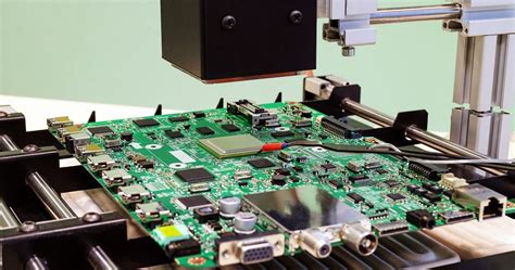
Quality assurance integrates automated optical inspection (AOI) and X-ray inspection to detect soldering defects or misalignments. These systems leverage machine learning to improve accuracy, reducing human error in PCBA validation.
As industries demand higher reliability, techniques like conformal coating protect assemblies from environmental stressors, extending product lifespans in harsh applications. Manufacturers also adopt modular production lines, allowing rapid reconfiguration for diverse PCB assembly requirements, from low-volume prototypes to mass production.
The shift toward eco-friendly practices further influences technique selection, with lead-free soldering and halogen-free substrates gaining prominence. These innovations collectively enhance yield rates while aligning with global sustainability standards.
Key Design Considerations for PCBAs
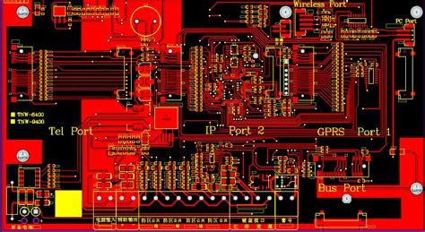
Effective PCBA design requires balancing technical precision with practical manufacturing requirements. A primary focus lies in optimizing component placement to minimize signal interference and ensure thermal efficiency. Engineers must prioritize PCB assembly compatibility by selecting components that align with automated pick-and-place machinery tolerances, reducing errors during high-volume production.
Another critical factor involves thermal management strategies, such as incorporating heat sinks or thermal vias, to prevent overheating in densely packed circuits. Material selection also plays a pivotal role—choosing substrates with appropriate dielectric properties ensures signal integrity, especially in high-frequency applications like 5G modules or IoT sensors.
Design for manufacturability (DFM) principles are indispensable, as they bridge the gap between theoretical schematics and practical PCBA execution. This includes adhering to clearance rules, avoiding acute angles in traces, and ensuring solder mask alignment. Additionally, designers must account for testability by integrating test points for in-circuit testing (ICT) or boundary scan protocols, streamlining quality assurance processes.
Finally, collaboration between design and PCB assembly teams ensures early identification of potential bottlenecks, such as incompatible component footprints or soldering challenges. By addressing these considerations, manufacturers achieve robust, scalable designs that meet evolving demands in automotive, consumer electronics, and industrial systems.
Optimizing Assembly Processes in PCBA
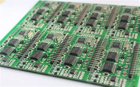
Efficient PCBA manufacturing relies on refining PCB assembly workflows to balance speed, precision, and cost-effectiveness. Central to this optimization is the adoption of automated surface-mount technology (SMT), which enables high-speed placement of miniature components with micron-level accuracy. Modern assembly lines integrate vision-guided robotic systems to handle complex layouts, reducing human error and rework rates. For mixed-technology boards, combining SMT with through-hole assembly requires precise thermal profiling to prevent solder joint defects during reflow soldering.
Transitioning to modular production setups allows manufacturers to adapt quickly to design changes, particularly for IoT or automotive applications demanding rapid prototyping. Implementing lean manufacturing principles—such as just-in-time component sourcing—minimizes inventory costs while maintaining production continuity. Advanced PCBA workflows also leverage real-time data analytics to monitor equipment performance, identifying bottlenecks in pick-and-place or soldering stages.
Critical to process optimization is rigorous design for manufacturability (DFM) analysis. Collaborating early with design teams ensures component spacing, pad geometries, and thermal requirements align with assembly capabilities. Post-assembly, automated optical inspection (AOI) and X-ray testing validate solder quality, creating a closed-loop feedback system for continuous improvement. By harmonizing these strategies, manufacturers achieve shorter lead times and higher yields—key drivers in today’s fast-evolving electronics sector.
Quality Control Methods for PCBA
Effective quality control is critical in PCBA production to ensure reliability and performance in end-use applications. Modern techniques begin with incoming inspection of components, verifying specifications against design requirements to prevent defects at the source. During PCB assembly, automated optical inspection (AOI) systems scan solder joints and component placement with micron-level precision, flagging issues like misalignments or insufficient solder. For high-density boards, X-ray inspection complements AOI by revealing hidden flaws such as voiding in ball grid arrays (BGAs).
Functional testing remains a cornerstone, where assembled boards undergo rigorous electrical validation under simulated operating conditions. Environmental stress screening (ESS), including thermal cycling and vibration tests, further ensures durability in demanding sectors like automotive or aerospace. Statistical process control (SPC) tools analyze production data to identify trends, enabling proactive adjustments to PCBA workflows.
Compliance with industry standards like IPC-A-610 and ISO 9001 provides a structured framework for consistency. By integrating these methods, manufacturers minimize rework, reduce costs, and align with the evolving demands of IoT and smart devices—key drivers of modern PCB assembly innovation.
Modern PCBA Applications in IoT Devices
The rapid growth of IoT devices has positioned PCBA (Printed Circuit Board Assembly) as a cornerstone of smart technology ecosystems. From wearable health monitors to industrial sensors, modern IoT solutions rely on advanced pcb assembly techniques to achieve compact designs, energy efficiency, and seamless connectivity. Miniaturization remains a critical focus, with high-density interconnects (HDIs) and flexible substrates enabling pcba integration into space-constrained devices like smart thermostats and asset-tracking tags.
Innovations in pcb assembly processes, such as automated optical inspection (AOI) and 3D solder paste inspection, ensure reliability in harsh environments—essential for agricultural IoT sensors exposed to moisture or temperature fluctuations. Additionally, low-power PCBAs with optimized signal integrity are driving advancements in battery-operated devices, including smart locks and environmental monitoring systems.
The rise of edge computing in IoT further underscores the importance of pcba durability and thermal management. Manufacturers now employ advanced materials like ceramic-filled laminates and embedded cooling solutions to handle increased processing demands. These developments not only enhance device performance but also align with evolving standards for data security and wireless interoperability, ensuring seamless integration into broader IoT networks. As IoT applications expand, the synergy between pcb assembly innovations and smart device requirements continues to redefine possibilities in consumer and industrial markets alike.
Automotive Electronics and PCBA Integration
The integration of PCBA (Printed Circuit Board Assembly) into automotive systems has become a cornerstone of modern vehicle design. As vehicles evolve into sophisticated electromechanical platforms, pcb assembly techniques must address unique challenges such as extreme temperature fluctuations, vibration resistance, and long-term reliability. Advanced PCBA designs now incorporate high-density interconnects and ruggedized components to ensure optimal performance in harsh automotive environments.
Key applications include engine control units (ECUs), advanced driver-assistance systems (ADAS), and infotainment modules. These systems rely on precision pcb assembly to manage complex signal routing and power distribution. For instance, automotive-grade soldering and conformal coatings are critical for preventing corrosion in moisture-prone areas. Additionally, the shift toward electric vehicles (EVs) demands PCBA solutions that support high-voltage battery management and fast-charging infrastructure.
To meet stringent safety standards, manufacturers employ automated optical inspection (AOI) and X-ray testing during pcb assembly, ensuring defect-free production. Innovations like embedded sensors and flexible circuits further enhance integration, enabling compact designs without compromising functionality. As automotive electronics continue to prioritize connectivity and autonomy, PCBA technologies will remain central to achieving scalable, efficient, and reliable vehicle architectures.
Consumer Electronics Innovations via PCBA
The rapid evolution of PCBA (Printed Circuit Board Assembly) technologies has become a cornerstone of innovation in consumer electronics, enabling smarter, smaller, and more energy-efficient devices. Advanced pcb assembly techniques, such as high-density interconnect (HDI) layouts and flexible PCB integration, allow manufacturers to pack more functionality into compact designs—critical for wearables, foldable smartphones, and ultra-thin laptops. For instance, modern wearables leverage pcba advancements to incorporate biometric sensors and low-power communication modules without compromising battery life.
Additionally, the shift toward IoT-enabled consumer products relies heavily on optimized pcb assembly processes. Smart home devices, from voice assistants to connected appliances, utilize multilayer PCBA designs to support wireless protocols like Wi-Fi 6 and Bluetooth 5.0. These innovations not only enhance user experiences but also streamline manufacturing scalability through automated soldering and precision component placement.
Thermal management solutions, such as embedded heat sinks and advanced substrate materials, further highlight how pcba refinements address performance challenges in high-power devices like gaming consoles and 4K streaming gadgets. As consumer demand for seamless connectivity and sustainability grows, pcb assembly techniques continue to evolve, balancing durability with eco-friendly material choices—a trend poised to redefine next-generation electronics.
How Innovations Drive PCBA Efficiency
Modern advancements in PCB assembly processes are revolutionizing manufacturing efficiency, enabling faster production cycles while maintaining rigorous quality standards. The integration of automated optical inspection (AOI) systems ensures precise detection of defects during PCBA, reducing manual inspection time by up to 70%. Additionally, AI-driven algorithms optimize component placement accuracy, minimizing material waste and rework rates.
Innovative surface-mount technology (SMT) advancements, such as ultra-fine-pitch soldering, allow denser circuitry layouts without compromising reliability. This is particularly critical for compact IoT devices and automotive electronics, where space constraints demand high-density PCBA designs. Furthermore, smart factories leveraging Industry 4.0 principles employ real-time data analytics to monitor assembly lines, predicting equipment maintenance needs and preventing unplanned downtime.
The adoption of eco-friendly materials, including halogen-free substrates and lead-free solder alloys, aligns with global sustainability goals while enhancing thermal performance in PCB assembly. Collaborative robotics, or cobots, further streamline workflows by handling repetitive tasks, freeing engineers to focus on complex problem-solving. These innovations collectively reduce production costs by 15–25% and accelerate time-to-market, ensuring PCBA remains at the forefront of modern electronics manufacturing.
Conclusion
As technological demands evolve across industries, PCBA remains the cornerstone of modern electronics manufacturing. The integration of advanced design methodologies and precision-driven PCB assembly processes has elevated production standards, enabling seamless applications in IoT ecosystems, automotive systems, and smart consumer devices. By prioritizing thermal management, component miniaturization, and automated testing, manufacturers achieve higher reliability while meeting stringent quality benchmarks.
The shift toward flexible manufacturing systems underscores the importance of adaptability in PCBA workflows, particularly for high-mix, low-volume production. Innovations such as AI-powered inspection tools and real-time data analytics further enhance error detection rates and process optimization, reducing time-to-market for cutting-edge products. From automotive ADAS modules to wearable health monitors, the convergence of PCB assembly excellence and application-specific engineering continues to redefine performance boundaries.
Ultimately, the future of PCBA hinges on balancing cost-efficiency with technological sophistication—a dual focus that ensures scalability without compromising on the precision required for next-generation electronics. As industries embrace smarter, interconnected solutions, the role of PCB assembly in enabling these advancements will only grow more pivotal.
Frequently Asked Questions
What distinguishes PCB assembly from PCBA?
PCB assembly refers to the process of populating a bare circuit board with components, while PCBA (Printed Circuit Board Assembly) describes the complete, functional unit after soldering and testing. The latter includes both the physical board and its integrated electronic elements.
How do design considerations impact PCBA reliability?
Critical factors like thermal management, component spacing, and material selection directly affect performance. Poor trace routing or inadequate heat dissipation can lead to premature failure, especially in high-density applications like IoT devices or automotive systems.
What quality control methods ensure PCBA consistency?
Automated optical inspection (AOI), X-ray testing, and functional circuit testing are standard. Manufacturers also employ statistical process control (SPC) to monitor solder paste application and component placement accuracy during PCB assembly.
Why is PCBA vital for modern consumer electronics?
Advanced PCBA techniques enable miniaturization and energy efficiency, supporting features like flexible circuits in wearables and high-speed signal processing in smartphones. Innovations in surface-mount technology (SMT) further enhance production scalability.
How do automotive applications demand specialized PCBA?
Vehicles require boards resistant to vibration, temperature extremes, and electromagnetic interference. Rigorous testing protocols, such as AEC-Q100 compliance, ensure PCBA reliability in safety-critical systems like ADAS or EV battery management.
Explore Professional PCBA Solutions Today
For tailored PCB assembly services that align with industry standards, please click here to consult our engineering team for prototyping or large-scale production needs.


