Precision Control in PCB Cloning: Techniques and Best Practices
Abstract
Printed Circuit Board (PCB) cloning, also known as PCB copy or reverse engineering, is a process that involves replicating an existing PCB design for repair, improvement, or legacy system maintenance. One of the most critical aspects of PCB cloning is precision control, as even minor deviations can lead to functional failures. This article explores the key factors influencing PCB cloning accuracy, including scanning resolution, layer alignment, trace width consistency, and component placement. Additionally, we discuss advanced techniques such as high-resolution imaging, automated optical inspection (AOI), and computer-aided design (CAD) verification to enhance precision. Finally, best practices for minimizing errors and ensuring high-quality PCB replication are presented.
1. Introduction
PCB cloning is widely used in electronics manufacturing, repair, and research. However, achieving high precision in the copied PCB is challenging due to factors such as material differences, manufacturing tolerances, and measurement errors. This paper examines the methodologies and technologies used to control precision in PCB cloning, ensuring that the replicated board matches the original in functionality and reliability.
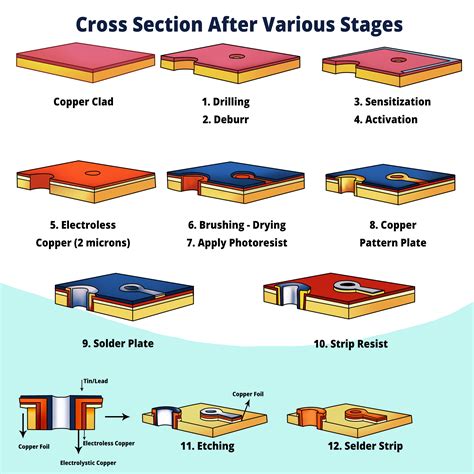
2. Key Factors Affecting PCB Cloning Precision
2.1 Scanning and Imaging Resolution
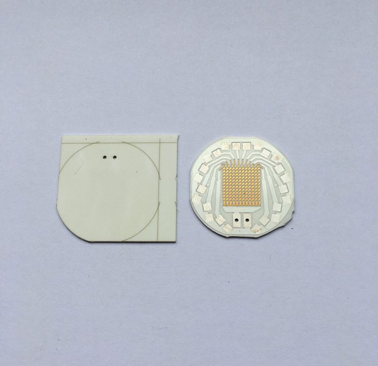
The first step in PCB cloning is obtaining a high-resolution scan of the original board. The scanning resolution directly impacts the accuracy of trace and pad reproduction.
- Optimal DPI (Dots Per Inch) Selection:
- For single-layer PCBs, 600–1200 DPI is usually sufficient.
- For multi-layer PCBs, especially those with fine-pitch components, 2400 DPI or higher is recommended.
- 3D Scanning for Depth Analysis:
- Laser scanning or structured light imaging helps capture solder mask thickness and via depths.
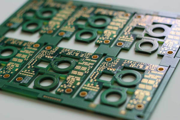
2.2 Layer Alignment in Multi-Layer PCBs
Misalignment between layers can cause short circuits or open connections. Techniques to ensure proper alignment include:
- Fiducial Mark Matching: Using reference points on each layer for alignment.
- Optical Registration Systems: Automated systems that align layers based on scanned images.
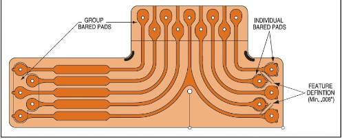
2.3 Trace Width and Spacing Consistency
Even slight variations in trace width can affect impedance and signal integrity.
- High-Precision Etching: Using chemical or laser etching to maintain trace dimensions.
- Automated Optical Inspection (AOI): Verifying trace widths against the original design.
2.4 Component Placement Accuracy
Incorrect component positioning can lead to assembly issues.
- Pick-and-Place Machine Calibration: Ensuring machines place components within ±0.05 mm tolerance.
- X-Ray Inspection: Verifying hidden connections (e.g., BGA components).

3. Advanced Techniques for Precision Control
3.1 High-Resolution Imaging and CAD Reconstruction
- Image Enhancement Algorithms: Reducing noise and improving edge detection.
- Vectorization Tools: Converting scanned images into CAD files with precise dimensions.
3.2 Automated Optical Inspection (AOI)
- Defect Detection: Identifying missing traces, shorts, or misaligned vias.
- Comparison with Original Design: Overlaying cloned PCB images with reference files.
3.3 Electrical Testing and Signal Integrity Verification
- Continuity Testing: Ensuring all connections match the original.
- Impedance Measurement: Verifying high-speed signal integrity.
4. Best Practices for High-Precision PCB Cloning
4.1 Pre-Cloning Analysis
- Document Original PCB Specifications: Record material type, layer stack-up, and critical tolerances.
- Non-Destructive Testing (NDT): Use X-ray or ultrasonic inspection to analyze internal structures.
4.2 Process Optimization
- Controlled Environment: Minimize dust and humidity during scanning and manufacturing.
- Multi-Stage Verification: Perform checks after scanning, etching, and assembly.
4.3 Post-Cloning Validation
- Functional Testing: Power up the cloned PCB and test all functionalities.
- Thermal and Stress Testing: Ensure reliability under operational conditions.
5. Conclusion
Precision control in PCB cloning is essential for producing reliable and functional replicated boards. By leveraging high-resolution imaging, automated inspection systems, and strict process controls, manufacturers can achieve near-identical reproductions of original PCBs. Future advancements in AI-based defect detection and nano-scale imaging may further enhance cloning accuracy.