Precision-Focused Electronics Assembly for Modern Manufactur
Key Takeaway
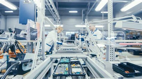
Modern electronics manufacturing hinges on precision-driven methodologies that align with evolving industrial requirements. Central to this is PCB assembly (PCBA), which integrates advanced techniques like automated optical inspection (AOI) and 3D solder paste monitoring to ensure micron-level accuracy. These processes not only enhance product reliability but also enable scalable production solutions, critical for industries transitioning to high-volume manufacturing.
| Factor | Technology | Impact |
|---|---|---|
| Precision Assembly | Laser Direct Imaging (LDI) | Reduces substrate alignment errors |
| Quality Assurance | X-ray inspection systems | Detects hidden solder joint defects |
| Scalability | Modular production lines | Supports rapid capacity adjustments |
Equally critical is the role of SMT assembly techniques in minimizing component placement deviations, particularly for fine-pitch ICs. As manufacturers prioritize zero-defect manufacturing, the adoption of Industry 4.0-compatible systems—such as IoT-enabled traceability platforms—ensures seamless integration of electronics assembly services into smart factories. This convergence of PCB assembly innovation and automated workflows underscores the sector’s shift toward data-driven, agile production ecosystems.
Precision in Electronics Assembly
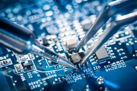
Achieving precision in electronics assembly requires meticulous attention to detail across every stage of PCB assembly and PCBA workflows. Modern manufacturing demands sub-millimeter accuracy in component placement, soldering, and testing to ensure optimal functionality in high-performance devices. Advanced optical inspection systems and automated pick-and-place machines now enable microscopic tolerances—critical for applications ranging from medical devices to aerospace systems.
"A single misaligned resistor or solder bridge can compromise an entire assembly. Partnering with a provider that adheres to IPC-A-610 standards ensures defect rates remain below 0.1%."
The integration of PCBA processes with real-time quality analytics further enhances precision. Techniques like 3D solder paste inspection and X-ray verification identify flaws invisible to the naked eye, while traceability systems track each component from procurement to final testing. For industries requiring miniaturization, such as IoT or wearables, laser-assisted PCB assembly achieves micron-level precision without thermal damage.
Scalability remains a key consideration—high-precision workflows must balance speed with accuracy, particularly when transitioning from prototyping to mass production. By combining rigid process controls with adaptive manufacturing technologies, manufacturers can meet both exacting quality benchmarks and evolving industrial demands.
Modern Manufacturing Quality Control
In today’s high-stakes industrial landscape, quality control stands as the backbone of effective electronics assembly services. Rigorous inspection protocols, powered by AI-driven analytics and real-time monitoring systems, ensure that every PCBA (Printed Circuit Board Assembly) meets exacting standards. Automated optical inspection (AOI) and X-ray testing are now integral to identifying micro-defects in PCB assembly, from solder joint integrity to component alignment, minimizing post-production failures.
Scalability demands further innovation: statistical process control (SPC) tools track variances across high-volume production runs, while traceability frameworks link each PCBA unit to its manufacturing lineage. This dual focus on precision and accountability not only reduces waste but also aligns with Industry 4.0’s emphasis on data-driven decision-making. By integrating advanced PCB assembly processes with adaptive quality systems, manufacturers achieve faster time-to-market without compromising reliability—a critical balance for sectors like aerospace, medical devices, and automotive electronics.
Transitioning seamlessly into scalable solutions, modern quality systems are designed to evolve alongside emerging technologies, ensuring compliance with international certifications such as ISO 9001 and IPC-A-610. This proactive approach future-proofs manufacturing workflows while maintaining the integrity of electronics integration methods.
Scalable Electronics Production Solutions
Modern manufacturing demands production systems that adapt seamlessly to evolving market needs while maintaining precision and cost-efficiency. Scalable electronics production solutions bridge this gap by offering flexible frameworks that expand or contract based on project requirements. Central to this scalability is the integration of PCB assembly (PCBA) processes optimized for variable batch sizes, from prototyping to high-volume runs. Advanced modular workflows enable manufacturers to reconfigure assembly lines swiftly, minimizing downtime and maximizing resource utilization.
The rise of automated PCB assembly technologies, including AI-driven pick-and-place systems and real-time quality monitoring, ensures consistent output across production scales. These systems support rapid transitions between surface-mount technology (SMT) and mixed-technology boards, critical for industries requiring both compact designs and robust performance. For instance, IoT device manufacturers leverage scalable PCBA solutions to manage seasonal demand spikes without compromising on solder joint integrity or component alignment accuracy.
Moreover, cloud-based production management platforms provide end-to-end visibility, allowing teams to synchronize PCB assembly timelines with material procurement and testing phases. This cohesion reduces lead times by up to 40% while maintaining defect rates below 0.5%. By aligning scalable electronics production with Industry 4.0 standards, manufacturers achieve not only operational agility but also future-proof their infrastructure against emerging technological shifts.
Advanced PCB Assembly Processes
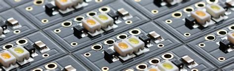
Contemporary manufacturing demands require PCB assembly (PCBA) systems that blend speed with microscopic accuracy. Modern facilities employ surface-mount technology (SMT) to place components as small as 01005 packages (0.4mm x 0.2mm) onto multilayer boards, achieving placement tolerances under 25µm. This precision is amplified by automated optical inspection (AOI) systems that perform 3D solder joint analysis at rates exceeding 20,000 components per hour, ensuring defect rates remain below 50 parts per million.
The shift toward Industry 4.0 has introduced adaptive assembly lines where PCBA workflows integrate real-time data from IoT-enabled machinery, enabling dynamic adjustments to thermal profiles during reflow soldering. Such systems maintain peak temperatures within ±1.5°C across entire production batches, critical for lead-free SAC305 alloys. For high-density interconnect (HDI) designs, manufacturers now utilize laser-drilled microvias with aspect ratios up to 12:1, supporting 20+ layer stackups while minimizing signal loss.
Scalability is achieved through modular PCB assembly cells that can transition between prototype runs and full-scale production within 24 hours. This agility pairs with traceability systems that track individual components from feeder to final test, aligning with ISO 9001:2015 compliance standards. The result? Zero-defect manufacturing pipelines capable of delivering 99.95% yield rates even for complex mixed-technology assemblies.
Reliable Electronics Integration Methods
Achieving consistent performance in modern electronics manufacturing hinges on robust integration methodologies that bridge design intent with production reality. Central to this process is PCB assembly (PCBA), where component placement accuracy and solder joint integrity directly impact end-product reliability. Advanced manufacturers employ traceability protocols and automated optical inspection (AOI) systems to validate connections at micron-level tolerances, particularly for high-density interconnect (HDI) boards.
The integration of mixed-technology components—combining surface-mount devices (SMDs) with through-hole parts—demands specialized reflow profiling and selective soldering techniques. For mission-critical applications, conformal coating processes and environmental stress screening (ESS) ensure long-term resilience against thermal cycling and mechanical vibration. Emerging edge-bonding methods further enhance structural stability in flex-rigid PCBA configurations, addressing challenges in wearable tech and aerospace systems.
Scalability remains paramount, with modular assembly lines enabling seamless transitions between prototype validation and full-scale production. By aligning design-for-manufacturability (DFM) principles with real-time process analytics, manufacturers reduce integration errors by up to 62% while maintaining IPC-A-610 Class 3 standards. This systematic approach to electronics integration supports both low-volume customization and high-mix industrial automation requirements without compromising quality thresholds.
Cutting-Edge SMT Assembly Techniques
Modern PCB assembly relies on innovative surface-mount technology (SMT) to meet the demands of high-density, miniaturized electronics. By leveraging ultra-precision pick-and-place systems, manufacturers achieve component placement accuracies within ±25 microns, ensuring flawless integration even for micro-BGA and 01005 packages. Advanced PCBA workflows now incorporate AI-driven optical inspection (AOI) systems, which perform real-time defect detection at speeds exceeding 50,000 components per hour.
A critical advancement lies in the adoption of low-temperature soldering techniques, which reduce thermal stress on sensitive ICs while maintaining joint integrity. Hybrid SMT lines combining conductive epoxy bonding and laser reflow processes further enhance reliability for aerospace and medical-grade applications. To address scalability, modular assembly platforms enable rapid reconfiguration between prototype batches and high-volume production runs—a necessity for IoT and automotive sectors.
Transitioning seamlessly from design to production, modern SMT workflows integrate closed-loop feedback mechanisms. These systems correlate PCB assembly data with CAD models, automatically adjusting parameters like stencil pressure or solder paste volume. Such innovations not only streamline PCBA quality control but also align with Industry 4.0’s demand for data-driven manufacturing ecosystems. As component densities continue to rise, these techniques ensure that precision and efficiency remain at the core of electronics manufacturing.
High-Volume Manufacturing Trends
The shift toward high-volume manufacturing in electronics assembly services demands innovations that balance speed with precision. Modern facilities now integrate modular production lines and automated PCB assembly workflows to meet escalating global demand. By leveraging PCBA-optimized machinery, manufacturers achieve throughput rates exceeding 500,000 units daily without compromising quality control standards—a critical advantage in sectors like automotive and consumer electronics.
A key trend is the adoption of AI-driven optical inspection systems, which reduce defects in PCB assembly by analyzing solder joints and component alignment in real time. These systems complement scalable electronics production frameworks, enabling rapid reconfiguration for diverse product batches. Additionally, advancements in SMT assembly techniques support finer pitch components, essential for miniaturized devices.
However, high-volume operations face challenges, including supply chain synchronization and thermal management in densely packed PCBA designs. Forward-thinking manufacturers address these through predictive maintenance protocols and collaborative robotics, ensuring seamless integration with Industry 4.0 infrastructures. As demand grows, the ability to scale electronics integration methods while maintaining cost-efficiency will define competitive leadership in the sector.
Automated Assembly for Industry 4.0
The transition to automated assembly systems has become a cornerstone of manufacturing strategies aligned with Industry 4.0 objectives. By integrating robotics, IoT-enabled machinery, and AI-driven inspection tools, modern PCB assembly workflows achieve unprecedented levels of speed, accuracy, and traceability. These systems excel in handling complex PCBA tasks—from placing microcomponents with sub-millimeter precision to executing multi-stage soldering processes under controlled environmental conditions.
A key advantage lies in adaptive production scaling, where smart factories dynamically adjust output volumes without compromising quality control standards. For instance, automated optical inspection (AOI) systems paired with machine learning algorithms detect defects in PCB assemblies at rates exceeding 99.98% accuracy, significantly reducing rework cycles. This precision is particularly critical for applications requiring high-density interconnects or mixed-technology boards combining surface-mount (SMT) and through-hole components.
Moreover, Industry 4.0-ready PCBA lines leverage real-time data analytics to optimize material utilization and energy consumption, aligning with sustainable manufacturing imperatives. The seamless integration of automated pick-and-place systems with enterprise resource planning (ERP) software further ensures just-in-time component sourcing, minimizing production bottlenecks. As manufacturers confront growing demands for miniaturized electronics and shorter product lifecycles, these intelligent assembly frameworks provide the agility needed to maintain competitiveness in global markets.
Conclu
The evolution of electronics assembly services underscores the critical balance between precision engineering and adaptable manufacturing frameworks. As industries increasingly prioritize zero-defect tolerance and rapid scalability, PCBA (printed circuit board assembly) methodologies have become the backbone of modern production ecosystems. By integrating advanced PCB assembly workflows with automated optical inspection systems, manufacturers can ensure seamless transitions from prototyping to high-volume production, all while maintaining stringent quality benchmarks.
Emerging trends in Industry 4.0 further amplify the need for reliable electronics integration, where smart factory ecosystems leverage cutting-edge SMT assembly techniques to minimize human error and optimize throughput. This shift not only reinforces the importance of scalable electronics production solutions but also highlights the role of data-driven process optimization in sustaining competitive advantage. For businesses navigating complex supply chains, partnering with precision-focused PCB assembly providers remains a strategic imperative to meet evolving industrial standards and deliver end-products that align with global reliability expectations.
Ultimately, the convergence of PCBA innovation and agile manufacturing principles paves the way for resilient, future-ready production models capable of addressing both current and unforeseen technological demands.
Frequently Asked Questions
How does precision-focused assembly impact product reliability?
Precision in PCB assembly ensures micron-level component placement accuracy, directly affecting circuit performance and long-term durability. Automated optical inspection (AOI) systems validate every solder joint, minimizing defect rates below 50ppm in high-volume production.
What distinguishes PCBA from conventional PCB manufacturing?
While PCB refers to bare board fabrication, PCBA (Printed Circuit Board Assembly) integrates component mounting, soldering, and testing. Advanced SMT assembly techniques enable 0201 metric component placements, achieving 99.98% first-pass yield rates in Industry 4.0-compliant facilities.
Can scalable solutions maintain quality during production surges?
Modular electronics assembly services utilize configurable production lines with real-time process monitoring. This allows seamless scaling from 500 to 500,000 units while preserving <1% thermal variance in reflow soldering profiles.
How do automated systems address complex BGA assemblies?
Vision-guided pick-and-place robots achieve ±25µm repeatability for ball grid array (BGA) components. Combined with X-ray inspection, this ensures 100% electrical connectivity verification for mission-critical applications.
Discover Tailored Electronics Manufacturing Solutions
For optimized PCB assembly workflows meeting ISO 9001:2015 and IPC-A-610 Class 3 standards, explore our advanced capabilities. Click here to discuss your project’s technical requirements with our engineering team.


