Precision in PCB Design and SMT Assembly Processes
Key Takeaways
Achieving precision in PCB design and SMT assembly hinges on a holistic approach that integrates advanced techniques, material expertise, and rigorous quality control. A well-optimized PCB layout prioritizes signal integrity through careful trace routing, impedance matching, and minimization of electromagnetic interference (EMI). Material selection, such as high-TG substrates and low-loss dielectrics, directly impacts manufacturing accuracy, thermal stability, and long-term reliability in PCBA applications.
Modern SMT assembly faces challenges like component miniaturization and solder joint consistency, which demand precision solutions such as automated pick-and-place systems and laser-cut stencils for solder paste deposition. Effective thermal management—through strategic copper pours, heatsinks, or embedded cooling channels—ensures sustained performance in high-density electronics.
Quality assurance in PCB assembly relies on automated optical inspection (AOI), X-ray testing, and in-circuit testing (ICT) to detect defects at micron-level tolerances. Emerging trends, including AI-driven design tools and IoT-enabled SMT production lines, are reshaping workflows to reduce human error and accelerate time-to-market. By balancing innovation with meticulous process control, manufacturers can deliver PCBA solutions that meet the exacting demands of industries like aerospace, medical devices, and automotive electronics.
Fundamentals of Precision in PCB Design and SMT Assembly
Precision in PCB design and SMT assembly forms the backbone of modern electronics manufacturing, where even minor deviations can compromise performance and reliability. At the core of this process lies meticulous planning during the PCB layout phase, where factors like component placement, trace routing, and thermal management are optimized to minimize signal interference and ensure electrical stability. For instance, maintaining controlled impedance in high-frequency circuits requires precise calculation of trace widths and dielectric material properties, directly influencing signal integrity.
Material selection further dictates manufacturing accuracy. Substrates like FR-4, polyimide, or ceramic-based laminates each offer distinct thermal and mechanical properties. A comparative analysis of common materials is outlined below:
| Material | Thermal Conductivity (W/m·K) | Dielectric Constant (1 MHz) | Typical Application |
|---|---|---|---|
| FR-4 | 0.25 | 4.5 | Consumer Electronics |
| Polyimide | 0.52 | 3.5 | Aerospace, Flexible PCBs |
| Ceramic-Filled | 2.5 | 6.0 | High-Power Circuits |
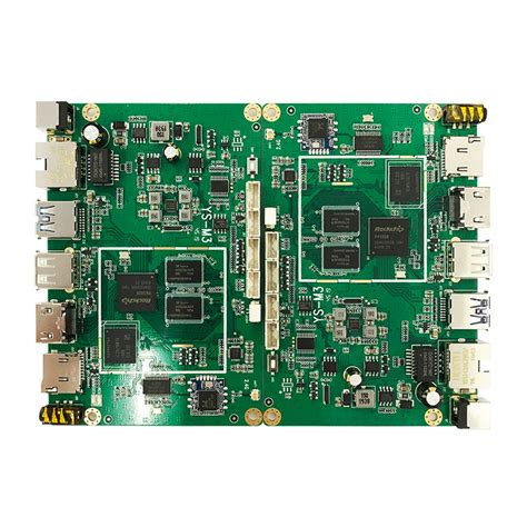
In SMT assembly, precision extends to solder paste application, component placement, and reflow profiling. Automated pick-and-place machines achieve placement accuracies within ±25 microns, critical for miniaturized components like 0201 resistors or QFN packages. However, variations in solder paste volume or reflow temperatures can lead to defects such as tombstoning or cold joints. To mitigate these risks, advanced inspection systems like automated optical inspection (AOI) and X-ray imaging are integrated into PCBA workflows.
"Precision in PCB design isn’t just about functionality—it’s about anticipating manufacturing variables to ensure seamless scalability."
A key tip for designers is to adopt design for manufacturability (DFM) principles early in the process. This includes adhering to clearance rules, optimizing pad geometries, and collaborating with PCB assembly partners to validate tolerances. For example, ensuring adequate spacing between components reduces the risk of solder bridging during reflow, particularly in dense PCBA layouts.
By harmonizing precise design practices with robust SMT assembly techniques, manufacturers can achieve repeatable quality, reduce rework costs, and deliver electronics that meet the stringent demands of industries like automotive, medical, and IoT.
Key Techniques for Optimizing PCB Layout and Signal Integrity
Achieving optimal PCB layout and signal integrity requires a meticulous approach to design, particularly in balancing electrical performance with manufacturability. A critical starting point is strategic component placement, which minimizes trace lengths and reduces electromagnetic interference (EMI). For high-speed circuits, maintaining controlled impedance through precise trace width and spacing is essential. Differential pair routing and proper grounding techniques, such as using ground planes or split planes, help mitigate noise and crosstalk. Additionally, adhering to design-for-manufacturing (DFM) guidelines ensures compatibility with PCB assembly processes, preventing issues like solder bridging or misaligned components during PCBA stages.
Layer stackup optimization plays a pivotal role in signal integrity, especially in multilayer boards. By carefully arranging power and signal layers, designers can reduce loop inductance and voltage drops. Incorporating via-in-pad technology or microvias in high-density interconnect (HDI) designs further enhances signal paths while conserving space. Thermal management must also be addressed early in the layout phase; strategic placement of thermal vias and heat sinks ensures even heat distribution, preventing hotspots that could degrade component reliability post-PCBA.
Material selection directly impacts performance, with low-loss dielectrics like Rogers or FR-4 hybrids preferred for high-frequency applications. Signal integrity simulations, such as SI/PI analysis, validate designs before prototyping, identifying potential reflections or timing errors. For mixed-signal systems, partitioning analog and digital sections and using guard traces or shielding can isolate sensitive circuits.
Finally, collaboration between design and PCB assembly teams is vital. Ensuring clear documentation, such as assembly drawings and a comprehensive bill of materials (BOM), streamlines the PCBA workflow. By integrating these techniques, manufacturers achieve repeatable precision, reducing rework and enhancing the reliability of modern electronics.
Material Selection and Its Impact on Manufacturing Accuracy
The choice of materials in PCB assembly and PCBA plays a pivotal role in determining manufacturing accuracy, directly influencing the performance and longevity of electronic devices. Substrate materials, such as FR-4, polyimide, or ceramic-based laminates, must align with the thermal, mechanical, and electrical demands of the design. For instance, high-frequency applications require low-loss dielectrics like Rogers materials to minimize signal attenuation, while flexible circuits demand polyimide substrates for their bend tolerance. The coefficient of thermal expansion (CTE) of these materials must closely match that of embedded components to prevent warping or solder joint fractures during thermal cycling, a critical factor in SMT assembly reliability.
Solder mask and surface finish selections further refine precision. Liquid photoimageable solder masks (LPISM) ensure precise aperture definition, reducing risks of bridging or tombstoning during reflow. Surface finishes like ENIG (Electroless Nickel Immersion Gold) or OSP (Organic Solderability Preservative) influence solderability and pad flatness, directly affecting placement accuracy in automated SMT processes. For high-density designs, immersion silver finishes offer superior planarity, enabling finer-pitch component placement.
Material compatibility with stencil printing is equally vital. Solder paste alloys (e.g., SAC305) must align with substrate and component metallurgies to avoid void formation or cold joints. Additionally, adhesives used for component bonding or underfill applications require precise viscosity control to prevent misalignment during curing. Advanced materials like low-temperature co-fired ceramics (LTCC) or metal-core PCBs address thermal management challenges, ensuring dimensional stability even in high-power applications.
Ultimately, material choices in PCB assembly and PCBA are a balancing act between electrical performance, thermal resilience, and manufacturability. Selecting substrates, finishes, and adhesives that harmonize with design specifications and assembly workflows minimizes defects, enhances yield rates, and ensures the final product meets stringent precision benchmarks.
Advanced SMT Assembly Challenges and Precision Solutions
Modern PCB assembly processes, particularly surface-mount technology (SMT), face escalating demands for precision as electronic devices shrink in size while increasing in complexity. One of the foremost challenges in SMT assembly is maintaining component placement accuracy at microscales, especially with ultra-fine-pitch components and high-density interconnects (HDIs). Misalignment during placement can lead to signal degradation, short circuits, or complete device failure. To address this, advanced pick-and-place machines equipped with vision systems and real-time feedback mechanisms ensure micron-level accuracy, even when handling components as small as 01005 packages.
Another critical challenge lies in solder paste deposition, where inconsistencies in volume or alignment directly impact PCBA reliability. High-precision stencil printing technologies, combined with laser-cut stencils and automated inspection systems, mitigate these risks by ensuring uniform paste application. Additionally, reflow profiling plays a pivotal role in achieving reliable solder joints. Optimized temperature curves prevent defects like tombstoning or voiding, particularly in mixed-technology boards combining SMT and through-hole components.
Thermal management during assembly further complicates SMT processes, as uneven heat distribution can warp substrates or damage sensitive components. Innovations such as automated thermal profiling and zone-controlled reflow ovens maintain consistent thermal conditions across the board. For high-power applications, the integration of thermally conductive adhesives and advanced underfill materials enhances structural stability and heat dissipation.
Quality assurance remains a cornerstone of precision-driven PCB assembly. Automated optical inspection (AOI) and X-ray inspection systems detect defects early, reducing rework costs and improving yield rates. These systems are increasingly augmented with AI-driven analytics to predict failure patterns and refine process parameters in real time.
Ultimately, overcoming advanced SMT assembly challenges requires a synergy of cutting-edge equipment, material science advancements, and data-driven process optimization. By prioritizing precision at every stage—from component placement to final inspection—manufacturers can deliver PCBA solutions that meet the rigorous demands of modern electronics.
Thermal Management Strategies for Enhanced Reliability in Electronics
Effective thermal management is a cornerstone of reliable PCB assembly (PCBA) and SMT processes, particularly as electronic devices demand higher power densities and miniaturization. Heat dissipation challenges arise from densely packed components, high-speed signal traces, and power-hungry ICs, which can compromise performance and longevity if unaddressed. To mitigate thermal stress, designers prioritize material selection, opting for substrates with high thermal conductivity, such as metal-core PCBs or ceramics, to efficiently transfer heat away from critical components. Additionally, optimizing copper pour layouts and incorporating thermal vias helps distribute heat evenly across the board, reducing localized hotspots.
In SMT assembly, component placement plays a pivotal role. High-power devices, like MOSFETs or processors, are strategically positioned to avoid clustering, ensuring adequate airflow and access to heat sinks. Advanced reflow soldering profiles are calibrated to minimize thermal shock during soldering, preserving the integrity of temperature-sensitive components. For PCBA systems operating in harsh environments, conformal coatings with high thermal resistance are applied to shield circuits from external heat sources.
Simulation tools, such as finite element analysis (FEA), enable precise modeling of heat distribution, allowing engineers to refine designs before prototyping. Real-time thermal imaging during testing further validates these models, ensuring alignment between theoretical and practical outcomes. Active cooling solutions, including heat sinks, fans, or liquid cooling systems, are integrated into the final design when passive methods fall short.
Finally, adherence to industry standards for thermal derating—reducing component power ratings under elevated temperatures—ensures long-term reliability. By combining robust design practices with rigorous validation, manufacturers achieve thermal stability, extending the lifespan of PCB assembly products while maintaining performance under demanding conditions.
Quality Control Processes in High-Accuracy PCB Manufacturing
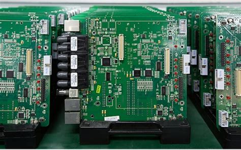
Ensuring precision in PCB assembly and PCBA (Printed Circuit Board Assembly) requires rigorous quality control (QC) protocols tailored to high-accuracy manufacturing. At every stage—from design validation to final inspection—processes are optimized to minimize defects and ensure adherence to stringent tolerances. Automated Optical Inspection (AOI) systems, for instance, scan boards for soldering flaws, misaligned components, or trace irregularities, leveraging high-resolution cameras and machine learning algorithms to detect sub-micron deviations. Similarly, X-ray inspection is employed to scrutinize hidden connections, such as ball grid arrays (BGAs), ensuring solder joint integrity in complex multilayer designs.
Electrical testing, including in-circuit testing (ICT) and flying probe testing, validates functionality by simulating real-world operating conditions. These tests identify opens, shorts, or parametric failures that could compromise performance. For high-reliability applications, environmental stress testing—such as thermal cycling or vibration testing—is integrated to assess durability under extreme conditions.
Material verification is equally critical. QC teams inspect raw materials, such as copper-clad laminates and solder masks, for consistency in thickness, thermal stability, and dielectric properties. Advanced SMT assembly lines incorporate real-time process monitoring, using sensors to track reflow oven temperature profiles and solder paste deposition accuracy. Statistical Process Control (SPC) tools analyze data trends to preemptively address deviations before they escalate.
Traceability systems, powered by barcode or RFID tagging, ensure full accountability across the PCBA supply chain. Every component’s origin, placement coordinates, and test results are logged, enabling rapid root-cause analysis in case of failures. By combining automated systems with human expertise, manufacturers achieve near-zero defect rates, aligning with the precision demands of industries like aerospace, medical devices, and automotive electronics. This multifaceted QC framework not only safeguards product reliability but also reinforces trust in PCB assembly as a cornerstone of modern electronics manufacturing.
Emerging Trends in Automated PCB Design and SMT Technologies
The evolution of PCB assembly (PCBA) processes is increasingly driven by automation, enabling unprecedented precision in both design and manufacturing. Modern automated design tools leverage artificial intelligence (AI) and machine learning (ML) to optimize PCB layouts for signal integrity, thermal performance, and component density. These systems analyze vast datasets to predict potential bottlenecks, such as electromagnetic interference (EMI) or power delivery issues, and propose corrective adjustments before prototyping. In SMT assembly, robotic pick-and-place systems now achieve micron-level accuracy, reducing placement errors and enhancing throughput. Advanced vision systems paired with real-time feedback loops ensure components are aligned correctly, even on ultra-fine-pitch packages.
A critical trend is the integration of design-for-manufacturability (DFM) principles directly into PCB design software. This minimizes discrepancies between digital models and physical boards, streamlining the transition from PCB design to PCBA. For instance, automated DFM checks flag issues like insufficient solder mask clearance or incompatible component footprints, which are vital for high-yield production. Additionally, additive manufacturing techniques are gaining traction, allowing for rapid prototyping of complex, multilayer boards with embedded passives or flexible substrates.
In SMT technologies, the shift toward high-speed modular assembly lines supports mixed-product manufacturing without extensive retooling. Innovations such as laser-assisted soldering and precision paste-injection systems address challenges in miniaturization, particularly for components like 01005 resistors or micro-BGAs. Furthermore, IoT-enabled PCBA lines now collect real-time data on process parameters—such as reflow oven temperature profiles—to dynamically adjust settings and maintain consistency across batches.
Sustainability is also shaping automation trends, with systems optimizing material usage to reduce waste in solder paste or copper etching. Meanwhile, advancements in automated optical inspection (AOI) and X-ray inspection ensure defects are identified early, preserving the reliability of high-density assemblies. As industries embrace Industry 4.0, the synergy between PCB design automation and SMT assembly technologies will continue to redefine precision, scalability, and efficiency in electronics manufacturing.
Conclusion
The evolution of PCB design and SMT assembly has underscored the necessity of precision-driven methodologies to meet the demands of modern electronics. By integrating advanced techniques such as automated optical inspection (AOI) and 3D solder paste inspection (SPI) into PCBA workflows, manufacturers can significantly enhance accuracy while minimizing defects. Critical to this process is the alignment of PCB layout optimization with signal integrity principles, ensuring that high-speed circuits operate reliably even in compact, multi-layered designs. Material selection further plays a pivotal role, as substrates with low thermal expansion coefficients and high glass transition temperatures improve both manufacturing consistency and long-term durability.
In SMT assembly, challenges like component miniaturization and fine-pitch soldering demand meticulous process control. Innovations such as laser-assisted reflow soldering and precision pick-and-place systems address these hurdles, enabling the reliable placement of micro-scale components. Additionally, robust thermal management strategies—such as embedded heat spreaders and thermally conductive adhesives—ensure that densely packed PCBA systems maintain operational stability under varying load conditions.
Quality assurance remains a cornerstone of high-accuracy manufacturing, with in-circuit testing (ICT) and X-ray inspection serving as indispensable tools for validating PCB assembly integrity. As automated design tools and AI-driven analytics continue to advance, the industry is poised to achieve unprecedented levels of precision, reducing time-to-market while elevating performance benchmarks. By prioritizing these interconnected disciplines, stakeholders can deliver electronics that not only meet but exceed the reliability and efficiency expectations of today’s interconnected world.
Frequently Asked Questions
What defines precision in PCB design and SMT assembly?
Precision in PCB design and SMT assembly refers to the meticulous alignment of design specifications, material choices, and manufacturing processes to ensure optimal electrical performance, mechanical stability, and reliability. This includes minimizing signal interference, ensuring accurate component placement, and adhering to tight tolerances during PCBA (Printed Circuit Board Assembly).
How does material selection impact manufacturing accuracy?
Material selection directly influences thermal stability, signal integrity, and solderability. For example, high-Tg (glass transition temperature) substrates reduce warping during SMT assembly, while copper weight and dielectric constants affect impedance control. Choosing the right materials ensures consistency in PCB assembly processes and minimizes defects.
What are common challenges in advanced SMT assembly?
Key challenges include microcomponent placement (e.g., 0201 or 01005 packages), solder paste deposition accuracy, and thermal profiling for lead-free soldering. Advanced techniques like automated optical inspection (AOI) and precision stencil design help mitigate these issues, ensuring high yields in PCBA workflows.
Why is thermal management critical in PCB design?
Effective thermal management prevents overheating, which can degrade component lifespan and performance. Strategies like thermal vias, heat sinks, and optimized copper pours are essential in high-density layouts. These measures are particularly vital in PCB assembly for power electronics and IoT devices.
How does quality control ensure reliability in PCB manufacturing?
Quality control involves rigorous testing, including electrical testing (e.g., flying probe), X-ray inspection for hidden solder joints, and environmental stress screening. These steps validate the precision of SMT assembly processes and ensure compliance with industry standards such as IPC-A-610.
What trends are shaping automated PCB design and SMT technologies?
Emerging trends include AI-driven design optimization, 3D-printed solder masks, and robotic pick-and-place systems with micron-level accuracy. These innovations enhance efficiency and scalability in PCB assembly, catering to demands for miniaturization and faster time-to-market.
Explore Professional PCB Assembly Solutions
For tailored PCBA services that prioritize precision and reliability, please click here to explore advanced manufacturing solutions.


