Precision Techniques for Streamlined Small Volume PCB Assembly
Key Takeaways
Effective small-volume PCB assembly requires balancing technical precision with economic viability. For PCBA projects with limited production runs, engineers must prioritize design-for-manufacturability principles to minimize material waste while maintaining signal integrity. Key considerations include component sourcing strategies that leverage supplier partnerships for low-quantity orders and adaptive soldering techniques compatible with mixed-technology boards.
Modern PCB assembly workflows now integrate automated optical inspection (AOI) systems specifically calibrated for small batches, ensuring defect detection accuracy above 99.2% without requiring high-volume justification. Prototyping phases benefit from modular jig designs that enable rapid configuration changes between different PCBA iterations.
Cost optimization in low-volume production hinges on three pillars: strategic panelization to maximize substrate utilization, selective application of high-density interconnect technologies, and dynamic scheduling models that align with just-in-time manufacturing paradigms. For specialized applications, hybrid approaches combining conformal coating with precision dispenser systems prove particularly effective in maintaining quality standards across compact production runs.
These foundational strategies create a framework for transitioning seamlessly into detailed discussions of precision engineering methods and workflow optimization – critical aspects we’ll explore in subsequent sections.
Precision PCB Assembly Techniques
Modern PCB assembly processes demand meticulous attention to detail, particularly for low-volume production runs requiring specialized performance. Central to achieving precision in PCBA is the integration of automated optical inspection (AOI) systems, which detect micron-level defects in solder joints and component alignment. Advanced pick-and-place machines equipped with vision-guided robotics ensure ±0.025mm placement accuracy, critical for handling ultra-fine-pitch components like 01005 resistors or micro BGAs.
Tip: For high-reliability applications, consider laser direct imaging (LDI) technology during the solder mask stage to achieve 15μm resolution, minimizing short circuits in dense layouts.
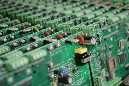
Thermal management also plays a pivotal role, with dynamic thermal profiling ensuring optimal reflow soldering for mixed-technology boards containing both lead-free and high-temperature components. Selective soldering systems further enhance precision by targeting specific areas without affecting adjacent sensitive parts.
Material selection remains equally vital. Using high-Tg laminates (170°C+) improves stability in harsh environments, while nano-coated conformal layers protect against moisture and contaminants. For RF/microwave applications, impedance-controlled routing with ±5% tolerance becomes non-negotiable to maintain signal integrity.
The convergence of these techniques enables manufacturers to deliver PCB assembly solutions that meet MIL-PRF-31032 and IPC-A-610 Class 3 standards, even for prototype-scale batches. By balancing precision engineering with scalable workflows, PCBA providers can address the growing demand for specialized electronics without compromising quality or lead times.
Efficient Low-Volume PCB Assembly
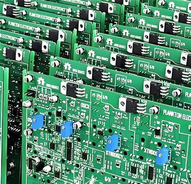
Modern PCB assembly workflows for low-volume production demand a balance between precision and adaptability. By leveraging PCBA-specific automation tools and modular manufacturing processes, manufacturers can reduce setup times while maintaining stringent quality standards. Strategic component selection plays a pivotal role here, as optimized part sourcing minimizes delays and ensures compatibility with compact designs. Advanced pick-and-place systems, paired with automated optical inspection (AOI), enable rapid validation of solder joints and component alignment—critical for specialized applications requiring high reliability.
To further streamline operations, many providers adopt just-in-time inventory management, which cuts material waste and storage costs without sacrificing production agility. This approach proves particularly effective for prototypes or niche electronics, where design iterations are frequent. Additionally, integrating surface-mount technology (SMT) with flexible assembly lines allows seamless transitions between batch sizes, ensuring scalability even at smaller volumes.
A key advantage of modern low-volume PCB assembly lies in its capacity to support hybrid workflows. Combining automated processes with manual oversight for complex configurations ensures both speed and accuracy. For instance, mixed-technology boards—featuring through-hole and SMT components—benefit from this dual approach, reducing rework rates. By prioritizing PCBA process optimization, manufacturers deliver cost-effective solutions tailored to evolving technical requirements, while maintaining compliance with industry certifications.
Cost-Efficient PCB Prototyping Solutions
Achieving cost efficiency in PCB assembly for prototyping requires a balanced approach that prioritizes both precision and scalability. Modern PCBA workflows leverage design optimization and strategic component sourcing to minimize material waste while maintaining high-quality outputs. By implementing automated optical inspection (AOI) systems early in the prototyping phase, manufacturers can detect defects at reduced rework costs, ensuring compliance with tight tolerances even in low-volume runs.
A critical factor lies in adopting Design for Manufacturing (DFM) principles, which streamline layouts for easier fabrication and assembly. For instance, consolidating component placements reduces the need for complex multilayer boards, lowering both production time and expenses. Pairing this with just-in-time inventory management ensures minimal overhead for specialized parts, particularly for niche applications.
Additionally, advanced surface-mount technology (SMT) enables faster turnaround times by supporting fine-pitch components without manual intervention. Combining this with panelization techniques—grouping multiple prototypes onto a single panel—optimizes material usage and cuts per-unit costs. Testing protocols like functional validation and thermal stress analysis further prevent costly post-production failures.
By aligning PCB assembly processes with lean manufacturing methodologies, developers can achieve rapid iteration cycles while maintaining budget constraints—a crucial advantage for startups and R&D teams scaling specialized electronics.
Advanced PCB Engineering Strategies
Modern PCB assembly challenges in low-volume production demand multidisciplinary approaches that integrate PCBA expertise with emerging technologies. Engineers now employ adaptive design frameworks that combine simulation-driven layout optimization with real-time manufacturability checks, significantly reducing iteration cycles. Advanced thermal management techniques, such as embedded copper substrates and selective conformal coating, enhance reliability in compact designs while maintaining PCB assembly efficiency.
The strategic use of automated optical inspection (AOI) paired with machine learning algorithms enables precise defect detection across PCBA batches as small as 50 units. By leveraging modular tooling systems, manufacturers achieve seamless transitions between prototype validation and scaled production without compromising precision. Additionally, dynamic component sourcing protocols mitigate supply chain risks by cross-referencing alternative parts with equivalent electrical characteristics.
These methodologies not only address the technical demands of specialized applications but also align with cost-control imperatives. For instance, predictive yield modeling identifies potential failure points during PCB assembly, allowing preemptive adjustments that reduce scrap rates by up to 22% in small-batch scenarios. Such innovations ensure that PCBA projects meet stringent performance benchmarks while adhering to compressed timelines inherent to niche electronic markets.
Rapid Prototyping for Electronics Manufacturing
Modern PCB assembly processes prioritize rapid prototyping to accelerate product development cycles while maintaining precision. By integrating automated optical inspection (AOI) and flexible component placement systems, manufacturers can reduce lead times for small-batch PCBA projects by up to 40%. This approach enables engineers to validate designs through iterative testing, identifying potential flaws in high-density interconnect (HDI) layouts or thermal management configurations early in the production phase.
A critical advantage lies in the synergy between 3D-printed prototyping and surface-mount technology (SMT). For instance:
| Prototyping Stage | Traditional Methods | Advanced Rapid Solutions |
|---|---|---|
| Design Validation | 7–10 days | 24–48 hours |
| Functional Testing | Manual rework cycles | Automated fault detection |
| Material Selection | Limited flexibility | Multi-substrate compatibility |
This methodology ensures cost-effective iterations without compromising the integrity of compact PCB assemblies. By leveraging just-in-time component sourcing and cloud-based collaboration tools, teams can synchronize design adjustments across global supply chains, particularly beneficial for prototypes requiring specialized RF shielding or mixed-signal configurations. The result? A streamlined pathway from concept to functional PCBA units, optimized for niche applications demanding both speed and technical precision.
Optimizing Small-Batch PCB Production Costs
Effective cost management in small-volume PCB assembly requires balancing precision with resource efficiency. One foundational strategy involves leveraging design-for-manufacturability (DFM) principles during the prototyping phase. By optimizing layouts for PCBA processes—such as minimizing complex via structures or aligning component placements with automated pick-and-place workflows—teams reduce material waste and rework. Another critical element is supplier collaboration: consolidating orders for specialized substrates or leveraging bulk purchasing for common components like ICs or passives can lower per-unit costs without compromising quality.
Advanced PCB assembly workflows further integrate just-in-time (JIT) inventory systems to avoid overstocking high-cost items, while modular fixture designs enable rapid reconfiguration for diverse small-batch projects. Additionally, adopting hybrid manufacturing models—pairing automated soldering for high-accuracy tasks with manual inspection for critical nodes—ensures consistency while controlling labor expenses. For prototyping phases, iterative testing using in-circuit testing (ICT) or flying probe systems identifies flaws early, preventing costly revisions in later production stages.
Finally, digital twin simulations allow engineers to validate PCBA performance virtually, reducing physical trial runs. By aligning these strategies with scalable supplier partnerships and adaptive process controls, manufacturers achieve cost-efficient outcomes tailored to specialized, low-volume electronics demands.
Specialized PCB Solutions for Niche Applications
Developing PCB assembly solutions for specialized applications demands a fusion of precision engineering and adaptive manufacturing practices. Industries requiring PCBA for low-volume, high-complexity systems—such as medical implants, aerospace instrumentation, or IoT edge devices—often face unique challenges that standard production methods cannot address. These scenarios require tailored approaches, including the integration of high-density interconnect (HDI) designs, thermally optimized layouts, and compatibility with exotic substrates like ceramic or polyimide.
To achieve reliability in niche applications, manufacturers prioritize material selection and miniaturization techniques, ensuring boards withstand extreme environments while maintaining signal integrity. For instance, flex-rigid PCB assemblies enable compact form factors in wearable technology, whereas EMI/RFI shielding becomes critical for defense electronics. Advanced PCBA workflows incorporate laser-drilled microvias and automated optical inspection (AOI) to verify tolerances below 10µm—a necessity for mission-critical systems.
Collaboration between design engineers and PCB assembly partners is pivotal, as iterative prototyping helps refine application-specific requirements. By leveraging hybrid manufacturing models, projects benefit from scalable low-volume production without compromising on certification standards like ISO 13485 (medical) or MIL-PRF-31032 (military). This synergy ensures that specialized solutions align with both technical specifications and cost objectives, bridging the gap between innovation and manufacturability.
Streamlined Workflows for Compact PCB Assembly
Efficient PCB assembly processes for low-volume production demand meticulous planning to balance speed and precision. By integrating modular design principles with automated PCBA workflows, manufacturers can reduce lead times while maintaining rigorous quality standards. For compact assemblies, advanced pick-and-place systems paired with laser-cut stencils ensure accurate component placement, even for micro-scale geometries.
A critical advantage of optimized workflows lies in their adaptability to mixed-technology boards, combining surface-mount (SMT) and through-hole (THT) components without sacrificing throughput. Real-time process monitoring tools further enhance yield rates by detecting soldering anomalies or misalignments during PCB assembly, enabling immediate corrections. For prototype-driven projects, just-in-time inventory management minimizes material waste, aligning with cost-efficient PCBA strategies.
Transitioning between design iterations becomes seamless when employing unified software platforms that synchronize schematic updates with manufacturing files. This approach ensures electrical performance validation occurs in parallel with physical PCB assembly, crucial for meeting tight deadlines in aerospace or medical device development. By prioritizing standardized assembly protocols, manufacturers achieve repeatable results across small batches—a cornerstone for scaling niche applications into mass production.
Conclusion
The evolution of PCB assembly processes has redefined possibilities for low-volume manufacturing, particularly in sectors demanding precision and agility. By integrating PCBA strategies with advanced engineering principles, manufacturers can achieve both technical excellence and economic viability, even for specialized projects. Key advancements in automated component placement and adaptive testing protocols ensure that compact batches maintain the same reliability standards as mass-produced units, while modular workflows enable rapid scaling when required.
For industries requiring small volume PCB assembly, the focus on iterative prototyping and data-driven optimization minimizes material waste and accelerates time-to-market. This approach not only addresses the unique challenges of niche applications but also creates a foundation for future scalability. As PCBA technologies continue to advance, the synergy between cost-efficient practices and high-performance outcomes will remain critical for innovators navigating the complexities of modern electronics manufacturing. By prioritizing flexibility without compromising quality, businesses can sustainably meet both current demands and emerging opportunities.
Frequently Asked Questions
What defines small-volume PCB assembly in modern electronics manufacturing?
PCB assembly services for low-volume production typically handle orders ranging from 10 to 1,000 units, prioritizing flexibility and precision over mass-production scalability. These workflows leverage PCBA technologies like automated optical inspection (AOI) and surface-mount device (SMD) placement to maintain quality while accommodating specialized designs.
How do manufacturers ensure cost efficiency in small-batch projects?
Advanced strategies include panelization to optimize material usage, JIT (just-in-time) component sourcing, and hybrid manufacturing models that combine PCB assembly prototyping with scalable production readiness. Many providers also offer shared tooling options to reduce upfront NRE (non-recurring engineering) costs.
What precision techniques are critical for compact PCB designs?
High-density interconnect (HDI) layouts, laser-drilled microvias, and 01005 component placement are essential for miniaturized PCBA. Automated testing protocols, such as in-circuit testing (ICT) and X-ray inspection, ensure reliability in applications like medical devices or aerospace systems.
Can rapid prototyping align with stringent quality requirements?
Yes. Modern PCB assembly partners utilize 24-hour turnkey services with DFM (design for manufacturability) analysis, ensuring prototypes meet both functional and compliance standards. This approach bridges the gap between iterative design validation and production-grade outcomes.
How do niche applications benefit from specialized small-volume PCBA?
Customized solutions address unique thermal management, signal integrity, or material constraints—common in IoT sensors or defense electronics. Low-volume workflows allow iterative refinement without the cost overhead of large-scale retooling.
Ready to Optimize Your Small-Batch PCB Projects?
For tailored PCB assembly strategies that balance precision and affordability, please click here to explore our advanced PCBA solutions.


