Precision Techniques in Circuit Card Assembly
Key Takeaways
When navigating PCB manufacturing for compact electronics, understanding core precision techniques becomes critical. Modern PCB manufacturing companies leverage advanced SMT soldering to handle high-density layouts, ensuring microscopic components adhere flawlessly to substrates. This process minimizes defects while optimizing PCB manufacturing cost through reduced material waste.
"Always verify that your assembly partner uses automated optical inspection (AOI) systems—these tools detect micron-level flaws invisible to the human eye, safeguarding reliability in high-stakes applications."
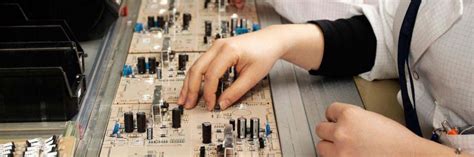
For micro-component placement, robotic systems achieve accuracies under 10µm, enabling designs that push the limits of miniaturization. Such precision directly impacts the PCB manufacturing business, as tighter tolerances translate to higher performance in devices like wearables or IoT sensors. Transitioning between assembly stages? Prioritize suppliers integrating high-speed pick-and-place machines with AOI feedback loops—this combo slashes production time while maintaining quality.
By balancing PCB manufacturing cost with cutting-edge techniques, you ensure boards meet both technical demands and budget constraints. Whether prototyping or scaling, these strategies form the backbone of reliable, future-ready electronics.
Advanced SMT Soldering for High-Density PCBs
When designing high-density PCB manufacturing solutions, you need soldering techniques that balance precision with thermal efficiency. Advanced surface-mount technology (SMT) soldering addresses this by enabling ultra-fine-pitch components to be placed on densely packed boards without compromising electrical integrity. Modern PCB manufacturing companies leverage laser-cut stencils and nitrogen-reflow ovens to achieve micron-level accuracy, ensuring solder joints remain void-free even in complex layouts.
A critical challenge lies in managing PCB manufacturing cost while maintaining quality. Automated paste dispensing systems reduce material waste, and predictive maintenance algorithms minimize downtime during high-volume production. For high-frequency applications, low-temperature solders with silver alloys enhance signal integrity, which is vital for 5G devices and IoT hardware.
To optimize your PCB manufacturing business, consider how advanced SMT processes integrate with downstream testing stages. Real-time thermal profiling, for instance, prevents warping in multilayer boards—a common issue in compact electronics. Industry benchmarks show that pairing these techniques with rigorous quality control can slash defect rates by over 60%, making your assembly line both efficient and scalable. By prioritizing precision at every stage, you ensure reliability without sacrificing performance in today’s shrinking electronic designs.
Automated Optical Inspection in PCB Assembly
When you’re managing PCB manufacturing workflows, ensuring defect-free production is non-negotiable. Automated Optical Inspection (AOI) systems act as the eyes of modern assembly lines, scanning boards at micron-level precision to detect soldering flaws, misaligned components, or missing parts. For PCB manufacturing companies, integrating AOI reduces human error by over 70%, directly lowering PCB manufacturing cost while maintaining compliance with industry standards like IPC-A-610.
Here’s how AOI optimizes quality control:
| Inspection Stage | AOI Advantage | Impact on PCB Manufacturing Business |
|---|---|---|
| Post-SMT Placement | Identifies tombstoning or skewed components | Minimizes rework time by 40% |
| Post-Reflow Soldering | Detects bridging or insufficient solder | Improves first-pass yield by 25% |
| Final Assembly | Verifies polarity and part orientation | Reduces field failure rates by 15% |
By deploying AOI early in the process, you avoid cascading defects that amplify PCB manufacturing cost downstream. Advanced systems use machine learning to refine defect recognition, adapting to new component geometries common in high-density designs. For startups in the PCB manufacturing business, modular AOI solutions offer scalability—ensuring quality without overinvesting in hardware.
Transitioning to AOI isn’t just about catching errors; it’s about building a data-driven feedback loop. Real-time analytics help you pinpoint recurring issues in solder paste application or pick-and-place accuracy, enabling continuous process refinement. This proactive approach ensures your PCB manufacturing operations stay competitive in markets demanding zero-defect electronics.
Micro-Component Placement for Compact Electronics
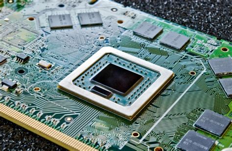
When designing compact electronics, achieving optimal PCB manufacturing outcomes hinges on mastering micro-component placement. Modern devices demand components as small as 01005 packages (0.4mm x 0.2mm), requiring PCB manufacturing companies to deploy high-precision pick-and-place machines with micron-level accuracy. These systems use advanced vision alignment to position resistors, capacitors, and ICs on densely packed boards, ensuring minimal signal interference and maximum space efficiency.
Balancing PCB manufacturing cost with precision is critical. While ultra-fine placement tools reduce human error, they require significant capital investment—a key consideration for any PCB manufacturing business aiming to scale. Automated workflows, combined with real-time feedback from AOI systems, help maintain consistency across batches, even as component sizes shrink.
To stay competitive, manufacturers must also address thermal management challenges. Miniaturized components generate concentrated heat, necessitating careful material selection and layout planning during assembly. By integrating laser-assisted soldering and adaptive algorithms, you can mitigate risks like tombstoning or misalignment, ensuring reliability in high-density designs.
As devices grow smaller, the interplay between precision placement and scalable PCB manufacturing processes becomes the cornerstone of innovation—enabling smarter wearables, medical implants, and IoT solutions without compromising performance.
Ensuring Reliability Through Precision Assembly
When building high-density electronics, PCB manufacturing demands microscopic accuracy to maintain functionality in compact designs. You achieve this through precision assembly processes that eliminate even sub-millimeter errors. Advanced PCB manufacturing companies leverage robotic pick-and-place systems calibrated to handle components as small as 01005 resistors, ensuring perfect alignment before soldering. These systems work in tandem with real-time thermal profiling to prevent warping or solder voids—common culprits behind circuit failures.
To balance PCB manufacturing cost and quality, manufacturers integrate automated optical inspection (AOI) at critical stages. AOI systems scan boards post-assembly, flagging defects like misaligned ICs or insufficient solder paste. This proactive approach reduces rework expenses while preserving the integrity of high-layer-count boards. For businesses scaling a PCB manufacturing business, investing in precision tools isn’t optional—it’s a strategic move to meet industry standards like IPC-A-610.
By prioritizing traceability and process control, you ensure every board meets rigorous reliability benchmarks. Whether it’s aerospace-grade durability or consumer electronics miniaturization, precision assembly bridges the gap between design intent and real-world performance.
Optimizing PCB Performance With AOI Systems
When refining PCB manufacturing processes, integrating automated optical inspection (AOI) systems becomes critical for balancing quality and PCB manufacturing cost. These systems scan boards at micron-level precision, identifying defects like solder bridges, misaligned components, or insufficient paste deposits that manual checks might miss. For PCB manufacturing companies, this translates to fewer post-assembly failures and reduced rework expenses—key factors in maintaining competitive pricing for high-volume orders.
AOI’s real-time feedback loops also enable faster adjustments during production. Imagine detecting a recurring soldering flaw early; you can recalibrate pick-and-place machines or reflow ovens immediately, minimizing downtime. This agility is particularly valuable in PCB manufacturing business models prioritizing rapid turnaround for IoT devices or wearables, where even minor defects compromise functionality in compact designs.
By pairing AOI with statistical process control (SPC) software, you gain actionable insights into yield rates and defect patterns. Over time, this data-driven approach optimizes material usage and labor allocation, further streamlining PCB manufacturing cost structures. Whether you’re prototyping or scaling production, AOI ensures each board meets exacting standards without inflating operational overhead—a non-negotiable in today’s high-stakes electronics market.
Innovations in Circuit Card Manufacturing Tech
As PCB manufacturing evolves, cutting-edge technologies are reshaping how high-density electronics are designed and produced. Leading PCB manufacturing companies now leverage laser-assisted soldering systems to achieve micron-level accuracy, enabling seamless integration of ultra-fine components on compact boards. By integrating AI-driven automated optical inspection (AOI), defects like micro-cracks or misalignments are detected in real time, reducing PCB manufacturing cost by minimizing rework. Advanced pick-and-place machines, equipped with vision-guided robotics, handle components as small as 01005 packages, ensuring precision even in high-speed assembly environments.
To stay competitive in the PCB manufacturing business, firms are adopting hybrid additive-subtractive processes, combining 3D printing for complex geometries with traditional etching for fine traces. These innovations not only enhance reliability but also accelerate prototyping cycles, critical for industries like wearables and IoT. Additionally, modular assembly lines now support rapid reconfiguration, allowing manufacturers to switch between low-volume, high-mix projects without compromising efficiency. By prioritizing precision techniques and smart automation, modern PCB manufacturing workflows deliver performance-driven solutions while addressing the growing demand for miniaturized, durable electronics.
High-Speed Assembly for Modern Electronics
When building compact, high-performance devices, PCB manufacturing relies on ultra-fast assembly lines to meet escalating demand. Modern PCB manufacturing companies leverage robotic pick-and-place systems that position components at speeds exceeding 50,000 placements per hour, ensuring rapid throughput without compromising accuracy. These systems integrate vision-guided alignment to handle sub-millimeter tolerances, critical for densely packed boards in smartphones or IoT devices.
Balancing PCB manufacturing cost with quality requires optimizing material usage and minimizing rework. High-speed assembly reduces cycle times, but thermal management becomes paramount. Advanced soldering techniques, like laser-assisted reflow, prevent warping in high-density interconnects while maintaining electrical integrity. For PCB manufacturing business models targeting mass production, investing in modular assembly lines allows scalability across product variants.
Transitioning from design to production, automated workflows synchronize CAD data with assembly machinery, eliminating manual errors. Real-time monitoring systems track yield rates, flagging defects early to avoid downstream bottlenecks. By aligning speed with precision, manufacturers achieve the dual goals of time-to-market acceleration and reliability—key drivers in today’s fast-evolving electronics landscape.
Future Trends in Circuit Card Assembly
As you look ahead, PCB manufacturing is poised to embrace smarter, more adaptive systems. Emerging technologies like AI-driven process optimization and modular assembly lines are redefining how PCB manufacturing companies balance precision with scalability. Expect to see greater integration of machine learning in defect prediction, reducing PCB manufacturing cost by minimizing material waste and rework cycles.
The shift toward flexible hybrid electronics will push boundaries in wearable tech and IoT devices, demanding ultra-thin substrates and advanced soldering techniques. Meanwhile, sustainability pressures are driving innovations in lead-free alloys and recyclable materials—critical factors for PCB manufacturing business models aiming to meet eco-certification standards.
Automation will deepen with collaborative robots (cobots) handling micro-component placement alongside human technicians, ensuring both speed and accuracy for high-mix production. As 5G infrastructure expands, expect tighter tolerances in RF circuit assembly, requiring real-time AOI systems with sub-micron measurement capabilities. These advancements won’t just streamline workflows—they’ll redefine what’s possible in miniaturized, high-reliability electronics.
Conclusion
When navigating the complexities of PCB manufacturing, it’s essential to recognize how precision techniques directly impact product reliability and performance. Whether you’re evaluating PCB manufacturing companies or optimizing your own PCB manufacturing business, understanding the interplay between advanced technologies and cost-efficiency becomes critical. Innovations like automated optical inspection (AOI) and high-speed micro-component placement not only enhance quality but also help manage PCB manufacturing cost by minimizing errors and material waste.
As compact electronics demand higher-density designs, the ability to integrate SMT soldering with rigorous testing protocols ensures your assemblies meet industry standards. By partnering with forward-thinking PCB manufacturing providers, you gain access to scalable solutions that balance precision with affordability. Looking ahead, advancements in AI-driven process optimization and sustainable materials will further redefine how businesses approach circuit card production. To stay competitive, prioritize suppliers who invest in cutting-edge tools while maintaining transparency in cost structures—this strategic alignment will position your projects for long-term success in an evolving market.
FAQs
How do PCB manufacturing companies ensure component placement accuracy?
Modern facilities combine high-speed assembly systems with automated optical inspection (AOI) to verify micron-level alignment. Advanced vision systems cross-check solder paste application and component orientation, minimizing human error in PCB manufacturing.
What factors influence PCB manufacturing cost for compact designs?
Material selection, layer count, and tolerances directly affect pricing. While micro-component placement and SMT soldering increase initial expenses, they reduce long-term failure rates. Partnering with experienced PCB manufacturing businesses optimizes cost-efficiency through bulk pricing and process refinement.
Why is AOI critical in high-density PCB manufacturing?
Automated inspection detects defects like solder bridges or misaligned chips before final testing. This step prevents costly rework, ensuring boards meet reliability standards for aerospace or medical devices.
Can small businesses access advanced PCB manufacturing technologies?
Yes. Many PCB manufacturing companies offer scalable solutions, from prototyping to mass production. Cloud-based quoting tools and modular assembly lines make precision techniques accessible regardless of order size.
Ready to Optimize Your Circuit Card Production?
For expert guidance on balancing PCB manufacturing cost with performance, please click here to explore tailored solutions from industry leaders.


