Precision Techniques in Rigid Flex PCB Assembly
Key Takeaways
Effective rigid flex PCB assembly relies on advanced techniques that balance precision and durability. Central to this process is laser cutting, which ensures micron-level accuracy in shaping complex circuit patterns. This method minimizes material stress, critical for maintaining the structural integrity of PCBA components. Equally vital are automated soldering techniques, leveraging robotic systems to achieve consistent joints across mixed rigid-flex interfaces, reducing human error in high-density layouts.
A cornerstone of successful PCB assembly is multilayer alignment, where optical registration systems align conductive layers within tolerances as tight as ±25µm. This step prevents signal loss and ensures compatibility with miniaturized electronic designs. Additionally, rigorous testing protocols validate thermal and mechanical resilience, addressing challenges posed by compact device architectures.
Innovations like 3D printed solder masks and AI-driven inspection tools are reshaping rigid flex PCBA, enabling faster prototyping and defect detection. By integrating these methodologies, manufacturers achieve high-yield production while meeting stringent reliability standards for aerospace, medical devices, and wearable tech. Each advancement underscores the importance of harmonizing precision engineering with scalable manufacturing workflows.
Rigid Flex PCB Assembly Overview
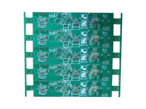
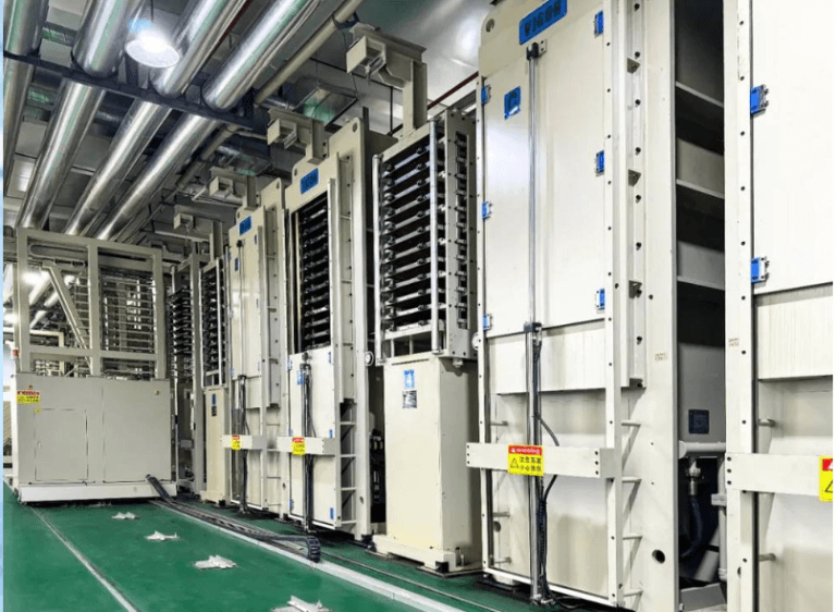
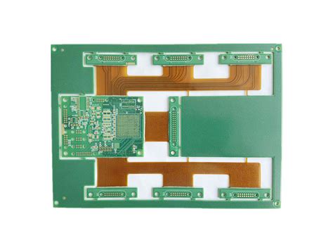
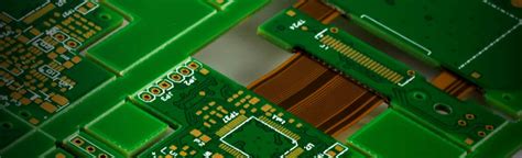
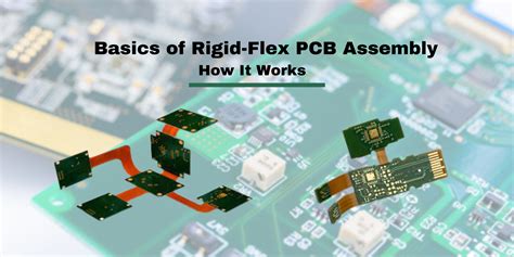
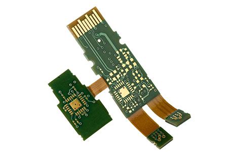
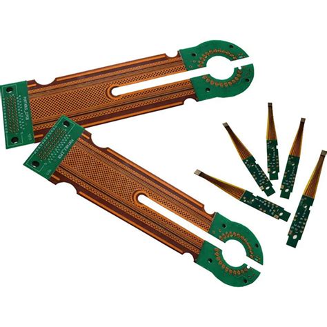
Combining the structural benefits of rigid and flexible substrates, rigid flex PCB assembly represents a critical advancement in modern electronics manufacturing. These hybrid boards integrate multilayer configurations to support high-density interconnects while maintaining mechanical resilience, making them ideal for aerospace, medical devices, and wearable technology. The PCBA process for rigid flex designs demands meticulous attention to material compatibility, thermal management, and layer alignment to prevent delamination or signal loss.
Key steps begin with selecting substrates that balance flexibility and durability, such as polyimide films paired with FR-4 laminates. Precision in PCB assembly hinges on advanced techniques like laser-drilled microvias and controlled impedance routing, which ensure signal integrity across bending zones. Manufacturers must also address challenges like coefficient of thermal expansion (CTE) mismatches during soldering, requiring specialized reflow profiles to avoid warping.
As the foundation for subsequent processes—such as laser cutting and automated soldering—the assembly phase sets the stage for reliability in compact devices. By harmonizing rigid and flex sections early in production, engineers mitigate risks of failure in dynamic applications, paving the way for innovations in miniaturized electronics.
Laser Cutting for PCB Precision
Laser cutting has become a cornerstone of modern PCB assembly, particularly for rigid flex PCBA designs requiring micron-level accuracy. Unlike traditional mechanical methods, laser systems enable non-contact material removal, minimizing stress on delicate substrates. This is critical for rigid flex boards, where alternating layers of rigid and flexible materials demand precise ablation depths to avoid damaging adjacent circuits.
Tip: When selecting a laser wavelength (e.g., CO₂ vs. UV), consider the substrate material. UV lasers excel at cutting polyimide flex layers without carbonization, ensuring cleaner edges for reliable interconnects.
| Key advantages of laser cutting in PCBA include: | Parameter | Laser Cutting | Mechanical Cutting |
|---|---|---|---|
| Precision Tolerance | ±10 μm | ±50 μm | |
| Kerf Width | 20–50 μm | 100–200 μm | |
| Heat-Affected Zone | <5 μm | 20–30 μm |
Automated laser systems also integrate with PCB assembly workflows, using CAD data to align cuts with pre-etched traces. For multilayer rigid flex boards, this ensures registration accuracy across layers, reducing risks of misalignment during lamination. Engineers often pair laser cutting with optical inspection to validate cut quality before proceeding to soldering or stacking phases.
Material compatibility remains a priority—laser parameters must adapt to varied substrates like FR-4, polyimide, or copper-clad laminates. By optimizing pulse duration and power, manufacturers achieve burr-free edges, essential for high-density interconnects in aerospace or medical PCBA applications.
Automated Soldering Techniques
Modern rigid flex PCB assembly relies heavily on automated soldering to achieve the precision required for high-density electronics. Unlike manual processes, automated systems use programmable machinery to ensure consistent thermal profiles and solder paste application, critical for maintaining electrical integrity in PCBA. Technologies like reflow soldering and selective soldering dominate this stage, with infrared or convection heating melting solder paste uniformly across complex rigid flex boards. These methods minimize human error, particularly when handling fine-pitch components or micro-BGA packages, where submillimeter alignment is essential.
A key advantage of automation lies in its ability to adapt to varying PCB assembly geometries. Advanced systems employ vision-guided robotics to adjust solder deposition in real time, compensating for warping or uneven surfaces common in rigid flex designs. Closed-loop feedback mechanisms further refine solder joint quality, reducing defects like bridging or cold joints by over 30% compared to manual techniques. For high-volume production, inline automated optical inspection (AOI) integrates seamlessly with soldering workflows, flagging anomalies before downstream processes.
As component miniaturization accelerates, the role of automated soldering in PCBA becomes indispensable. By combining speed with micron-level accuracy, these systems ensure reliability in applications ranging from medical implants to aerospace systems, where even minor soldering flaws can compromise entire assemblies. This precision dovetails with subsequent steps, such as multilayer alignment, to maintain structural and electrical coherence across the final product.
Multilayer Alignment Key Steps
Achieving precise multilayer alignment is critical in rigid flex PCB assembly, where even micron-level deviations can compromise performance. The process begins with registration marks etched onto each layer, serving as reference points for automated optical inspection (AOI) systems. Advanced PCBA workflows employ high-resolution cameras and machine vision algorithms to verify layer-to-layer alignment, ensuring conductive pathways match design specifications.
A key challenge lies in managing thermal expansion differences between rigid and flexible substrates during lamination. Manufacturers address this by calibrating pressure and temperature profiles to maintain dimensional stability. Laser-drilled microvias further enhance accuracy, enabling vertical interconnects across layers without misalignment risks.
For PCB assembly involving 10+ layers, sequential bonding techniques are paired with real-time monitoring to detect shifts during pressing. Cross-sectional imaging validates alignment post-lamination, while impedance testing confirms signal integrity. These steps are vital for applications like aerospace or medical devices, where multilayer rigidity-flex balance directly impacts reliability.
By integrating these methods, PCBA providers minimize rework and ensure consistent performance in high-density electronics, seamlessly transitioning to subsequent phases like soldering and final testing.
Compact Electronics Reliability
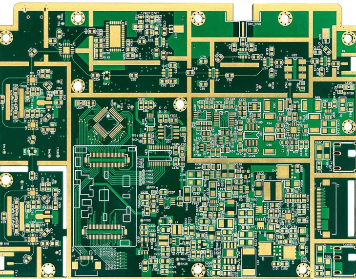
Achieving reliable performance in compact electronics demands meticulous attention to PCB assembly processes, particularly for rigid flex PCBA designs. The integration of rigid and flexible substrates introduces unique challenges, such as managing thermal expansion mismatches and minimizing mechanical stress at transition zones. To ensure longevity, manufacturers employ advanced automated optical inspection (AOI) systems to detect micro-cracks or misalignments that could compromise structural integrity. Additionally, controlled impedance routing and high-precision soldering are critical for maintaining signal integrity in densely packed circuits.
A key factor in reliability is the selection of materials with compatible coefficients of thermal expansion (CTE), which reduces stress during temperature fluctuations common in devices like wearables or medical implants. Rigid flex PCBA also benefits from conformal coating applications, which protect against moisture, dust, and chemical exposure. For mission-critical applications, rigorous environmental testing—including thermal cycling and vibration analysis—validates the assembly’s durability under extreme conditions. By balancing these technical considerations, PCB assembly teams deliver compact electronics that meet both performance benchmarks and long-term operational demands.
Advanced Rigid Flex PCB Tech
The evolution of rigid flex PCB assembly has introduced groundbreaking methodologies to address the complexities of modern electronics. Central to these advancements is the integration of embedded component technology, which allows active and passive components to be mounted directly within the substrate layers. This approach minimizes space consumption while enhancing signal integrity—a critical factor for PCBA in high-density applications like wearables and medical devices.
Innovations such as 3D laser ablation have refined the precision of creating microvias and fine-pitch traces, enabling seamless connectivity between rigid and flexible sections. Paired with automated optical inspection (AOI) systems, manufacturers can now detect submicron defects in real time, ensuring compliance with stringent reliability standards. Additionally, advancements in thermo-mechanical simulation tools optimize material selection, mitigating risks of delamination or thermal stress during operation.
These technologies collectively support the demand for PCB assembly processes that balance miniaturization with durability. By leveraging hybrid materials like polyimide-copper composites and adopting adaptive soldering profiles, PCBA workflows achieve consistent performance even in extreme environments. Such progress underscores the industry’s shift toward multifunctional, lightweight designs without compromising on the structural resilience required for next-generation electronics.
Precision PCB Assembly Methods
Achieving precision in PCB assembly demands a combination of advanced technologies and process control, particularly for rigid-flex designs that integrate both rigid and flexible substrates. Central to PCBA success is the use of high-resolution solder paste stencils, which ensure accurate deposition of conductive materials for micro-scale components. Automated optical alignment systems further enhance placement accuracy by compensating for substrate flexure during component mounting.
Critical to maintaining tolerances is the implementation of laser-etched fiducial markers, providing reference points for robotic assembly equipment to align multilayered circuits within ±25µm precision. For solder joint integrity, nitrogen-reflow ovens create oxygen-free environments, minimizing oxidation while enabling uniform thermal distribution across dissimilar materials. Post-assembly, 3D X-ray inspection verifies connections in hidden layers, detecting voids or cracks that could compromise reliability in compact devices.
These methodologies address the unique challenges of rigid-flex PCB assembly, where mismatched thermal expansion rates and dynamic bending requirements demand meticulous process validation. By integrating real-time monitoring and adaptive calibration, manufacturers ensure that PCBA outcomes meet the exacting standards of aerospace, medical, and wearable electronics applications.
Innovations in PCB Manufacturing
Recent advancements in PCB assembly technologies are reshaping how manufacturers approach rigid flex PCBA production. Automation now plays a central role, with robotic systems integrating AI-driven vision systems to detect micron-level defects during component placement. This reduces human error and ensures tighter tolerances, critical for high-density interconnects in modern electronics. Additionally, innovations like laser direct imaging (LDI) enable finer trace patterning, supporting the miniaturization trend without compromising signal integrity.
Another breakthrough lies in adaptive soldering systems, which dynamically adjust temperature profiles based on real-time thermal feedback. This is particularly vital for rigid flex PCBA, where mismatched thermal expansion between rigid and flexible layers can lead to joint failures. Advanced materials, such as low-loss dielectrics and high-ductility adhesives, further enhance reliability in harsh environments.
These innovations collectively address the growing demand for compact, high-performance devices, ensuring PCB assembly processes meet both precision and scalability requirements across industries like aerospace and medical technology.
Conclusion
The advancements in rigid flex PCB assembly underscore the importance of precision engineering in meeting the demands of modern electronics. By integrating laser cutting and automated soldering, manufacturers achieve unparalleled accuracy in PCBA processes, particularly for high-density interconnects and miniaturized components. These techniques not only enhance production efficiency but also mitigate risks associated with thermal deformation and mechanical stress in multilayer designs. Critical to success is the meticulous execution of multilayer alignment, which ensures signal integrity and structural stability in compact devices. As industries push for smaller, lighter, and more durable solutions, the role of PCB assembly innovations becomes pivotal in balancing performance with reliability. Future developments will likely focus on refining material compatibility and process automation to further streamline high-mix, low-volume production cycles. By prioritizing precision at every stage, the electronics sector can continue delivering robust solutions for applications ranging from aerospace to wearable technology.
FAQs
What distinguishes rigid flex PCB assembly from traditional PCB manufacturing?
Rigid flex PCBA combines rigid and flexible substrates, requiring specialized techniques like laser cutting and multilayer alignment to maintain structural integrity. This hybrid approach supports complex designs in compact electronics, unlike standard PCB assembly processes.
How does automated soldering enhance rigid flex PCB reliability?
Automated soldering ensures consistent joint quality, minimizing human error. By using precision-controlled reflow ovens and solder paste application, it addresses challenges like thermal stress on flexible layers, critical for high-density PCBA applications.
What role does laser cutting play in rigid flex PCB fabrication?
Laser cutting enables micron-level accuracy for shaping flexible circuits, reducing mechanical stress. This method is vital for creating intricate geometries in PCB assembly, ensuring compatibility with compact electronic enclosures.
Why is multilayer alignment critical in rigid flex PCBA?
Misalignment between rigid and flexible layers can cause signal loss or mechanical failure. Advanced optical alignment systems and registration marks ensure layer-to-layer precision, a cornerstone of reliable PCB assembly for aerospace and medical devices.
How are reliability issues tested in rigid flex PCB assemblies?
Testing includes thermal cycling, bend testing, and impedance checks. These validate performance under extreme conditions, ensuring the PCBA meets industry standards for durability in high-stress environments.
What innovations are shaping the future of rigid flex PCB technology?
Emerging trends include embedded components, 3D-printed circuits, and AI-driven quality control. These advancements streamline PCB assembly while enhancing precision for next-generation electronics.
Need Expert Rigid Flex PCB Assembly Services?
For tailored solutions in PCB assembly and PCBA, please click here to connect with our engineering team.