Principle of Parallel PCB Design
PCB design has become increasingly complex as the complexity of the devices they carry increases.For a long time,circuit designers have worked in isolation,then then transferred the completed schematics to PCB designers.PCB designers the completed their work independently and transferred the Gerber files to the PCB fabricator.These three groups worked in isolation,with lilttle communication.
With the increasing use of programmable devices in large BGA packages,high-density interconnects ,and timing-critical differential signaling,adopting this isolated PCB design approach is now catastrophic.A parallel development process allows multiple development steps to proces allow multiple development steps to proceed allows multiple development steps to proceed simultaneously,helping to ensure design success and avoid delays,additional costs,and rework.This article summarizes key principles for each stage of parallel PCB design.
This first step in pcb design is the concept phase.At this stage,the circuit designer and PCB designer should conduct a technical assessment together.This assessment should consider to following question:
1.What devices will be used?
2.what package will be used for the devices?
What is the pin count?What is the pin configuration?
3.Based on the cost-performance trade-off,how many PCB layers should be used?
4.What are the target values for parameters such as clock frequency and signaling speed?
Designers should also consider factors such as bus architecture,whether to use parallel or serial connections,and impedance matching strategies.Impedance mismatches can lead to reflection,ringing,and other undesirable interference.
Collaborative work
These PCB design consideration raise the question of communication as a key issue in successful pcb design.PCB design is no longer a one-person job but a team effort between different groups of engineers.Communication is a key theme throughout the PCB design process.The circuit design team must clearly communicate their design intent to the PCB design team and must participate in the process with a clear understanding of the capabilities and limitations of their PCB design tools.
With the increasing complexity of PCB routing and the increasing signal speeds,a collaborative PCB design approach can achieve better results than the traditional serial process(Figure 1).Separating component research and selection from the rest of the design process,as well as separating component research and selection from the rest of the design process,as well as separating the schematic capture,simulation,and layout stages,has long been a common approach.Therefore ,designer are best served by choosing tools and processes that facilitate data sharing.This is the only way for distributed design teams to leverage the benefits of parallel work and shorten the overall design cycle.
Key Principles of Parallel PCB design Figure:(a)Traditional serial PCB development processes result in long design cycles,limited information sharing,and escalating costs;(b)Parallel development processes allow multiple development processes to proceed simultaneously,helping ensure design success and avoiding delays,additional costs and rework.
Design Creation
During the design creation phase,engineers finalize components and generate libraries for them,which in turn speeds up schematic entry,During this phase,designers evaluate and select building blocks and can access manufacturer websites to search for datasheets and specifications.A better way to accomplish this is to select components directly during the schematic entry in this way,the process can be used as a method for experimentation.
During the schematic entry process,it is important for designers to be able to quickly add,delete,or change components(or even the entire design structure).For example,a designer developing a high-frequency filter for a mobile phone should set the passband and other filter parameters by experimenting with different capacitive and inductive values during schematic entry.
While creating the schematic ,PCB design tools also generate a netlist for the circuit behind the scenes.This netlist describes how the circuit’s components are connected and how subsequent placement and routing tools use it for PCB layout.
At this point,the desiger creates symbols and physical pinouts for so-called”large components,”such as FPGAs or other programmable devices.This is also when design constraints are captured ,a critical step that requires careful consideration,especially for subsequent processes.
In today’s PCB design,it’s best to follow the rules.In the past,manufacturing issues constrained everything,but now,as engineers strive to reduce PCB size while still making it manufacturable,everthing is subject to complex constrains.While design requirements may lead to large number of constrains,it’s important not to overconstrain the design.Relying more on simulation and analysis than simply constraining the design is a wiser approach.
During simulation,various design topologies can be tried,and component vendors typically address this issue by proving Spice models on the their websites,so it’s a good idea to search for them there.
Limitations of Detour Routing
Spice-based simulations, however,have limitations.They generate idealized signals that don’t necessarily represent real-world conditions.Real signals can contain noise and phase shifts that alter their authenticity.
National Instruments(NI)’s PCB design flow includes virtual instrumentation,which can be used with many NI PXI instruments to generate realistic signals,preserving their inherent nonlinearities. These signals can be captured in native file formats for use in Spice Simulations to verify circuit behavior.Furthermore,virtual prototypes provide feedback for component selection.
System-level simulation is also critical.It goes beyond modeling a single signal as it passes through the pcb ; it must examine how the signal behaves within a device or even across multiple board.Multi-gigabit signaling rates further complicate matters.The increasing popularity of serial bus architectures over parallel bus architectures requires PCB designers to simulate losses,coupled transmission line,and detailed via models.
Physical Implementation
After eliminating performance issues through simulation,the next step is to lay out and route the circuit to create a physical prototype.Layout ensures that circuit performance meets design specifications and that the board form factor matches the design form factor.Collaboration with mechanical engineers is essential at this stage.
During the layout and routing phase,the interconnections between components defined by the schematic can be implemented using the placement and routing tools offer some degree of automated placement and routing,but this is a double-edged sword.Designers need to use discretion when to manually route and when to use automated routing.Avoid automated placement and routing if a critical component needs to be placed,or if a connector must be placed on the edge the PCB.
The good news is that signal integrity issues can be proactively considered during layout and routing.This a phase that requires careful attention.A general rule of thumb is that if a signal takes more than one-third of its transition time to reach its destination,there may be a signal integrity issue along that path.

Design Constraints
During the design creation phase, engineers finalize components and generate libraries for them, which in turn speeds up schematic entry. During this phase, designers evaluate and select building blocks and can access manufacturer websites to search for datasheets and specifications. A better way to accomplish this is to select components directly during the schematic entry process. By implementing schematic entry in this way, the process can be used as a method for experimentation.
During the schematic entry process, it is important for designers to be able to quickly add, delete, or change components (or even the entire design structure). For example, a designer developing a high-frequency filter for a mobile phone should set the passband and other filter parameters by experimenting with different capacitive and inductive values during schematic entry.
While creating the schematic, PCB design tools also generate a netlist for the circuit behind the scenes. This netlist describes how the circuit’s components are connected and how subsequent placement and routing tools use it for PCB layout.
At this point, the designer creates symbols and physical pinouts for so-called “large components,” such as FPGAs or other programmable devices. This is also when design constraints are captured, a critical step that requires careful consideration, especially for subsequent processes.
In today’s PCB design, it’s best to follow the rules. In the past, manufacturing issues constrained everything, but now, as engineers strive to reduce PCB size while still making it manufacturable, everything is subject to complex constraints. While design requirements may lead to a large number of constraints, it’s important not to overconstrain the design. Relying more on simulation and analysis than simply constraining the design is a wiser approach.
During the design creation process, engineers should be aware of signal integrity issues that may arise later in the process. It’s best to consider signal integrity issues during the design entry and PCB layout phases. Of course, the design process must support this approach, as impedance mismatches cannot be addressed during the design entry phase.
Simulation is Key
Once the circuit design is complete and the schematic is drawn, functional verification is the next step, typically accomplished using simulation tools. The purpose of simulation isn’t to replace physical prototyping, but rather to avoid repeated prototyping, as simulation allows designers to identify design flaws that wouldn’t normally be discovered until prototyping is complete.
During simulation, various design topologies can be tried, and components from different manufacturers can be substituted to examine their impact on circuit performance. However, simulation is plagued by issues with model availability and validity. All common PCB design toolkits come with expensive model libraries, and it’s likely that a specific component isn’t included in the library. Component vendors typically address this issue by providing Spice models on their websites, so it’s a good idea to search for them there.
Limitations of Detour Routing
Spice-based simulations, however, have limitations. They generate idealized signals that don’t necessarily represent real-world conditions. Real signals can contain noise and phase shifts that alter their authenticity.
National Instruments (NI)’s PCB design flow includes virtual instrumentation, which can be used with many NI PXI instruments to generate realistic signals, preserving their inherent nonlinearities. These signals can be captured in native file formats for use in Spice simulations to verify circuit behavior. Furthermore, virtual prototypes provide feedback for component selection.
System-level simulation is also critical. It goes beyond modeling a single signal as it passes through the PCB; it must examine how the signal behaves within a device or even across multiple boards. Multi-gigabit signaling rates further complicate matters. The increasing popularity of serial bus architectures over parallel bus architectures requires PCB designers to simulate losses, coupled transmission lines, and detailed via models.
Physical Implementation
After eliminating performance issues through simulation, the next step is to lay out and route the circuit to create a physical prototype. Layout ensures that circuit performance meets design specifications and that the board form factor matches the design form factor. Collaboration with mechanical engineers is essential at this stage.
During the layout and routing phase, the interconnections between components defined by the schematic can be implemented using the placement and routing tools provided by any EDA vendor. All of these tools offer some degree of automated placement and routing, but this is a double-edged sword. Designers need to use discretion when to manually route and when to use automated routing. Avoid automated placement and routing if a critical component needs to be placed, or if a connector must be placed on the edge of the PCB.
The good news is that signal integrity issues can be proactively considered during layout and routing. This is a phase that requires careful attention. A general rule of thumb is that if a signal takes more than one-third of its transition time to reach its destination, there may be a signal integrity issue along that path.
Design Constraints
PCB layout and routing present many challenges, chief among which is ensuring that constraints are met. These constraints are used to address signal integrity issues, manufacturability issues, electromagnetic interference, thermal effects, or a combination of these.
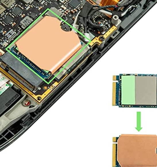
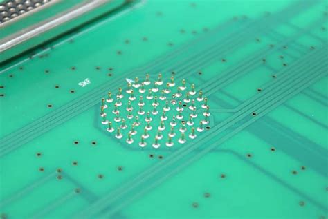
In addition to design constraints, PCB layout and routing is further complicated by numerous factors related to current device technologies. For example, advanced semiconductor packaging technologies such as chip-on-board (COB) can make routing extremely challenging. Current high-density packages can accommodate over 2,000 pins with a pitch of less than 0.65mm. Managing I/O and signal speeds in these packages can be challenging, and escape routing for these packages is a highly skilled task.
PCB layout for programmable logic devices presents another challenge. Some high-end PCB design toolkits, such as those from Altium and Mentor Graphics, offer tight integration with FPGA vendors’ design tools and can be used to integrate the FPGA and PCB design.
Historically, pin configuration for large FPGAs was typically performed by FPGA designers, without much consideration given to PCB layout. Now, it’s recognized that FPGAs with programmable I/O are the source of incoming and outgoing traces, making it much easier to modify the FPGA to accommodate PCB layout than to modify the PCB to match the FPGA’s I/O configuration.
Final Check
The final step before sending the PCB layout for fabrication is the final check. Signal integrity and timing must be checked to ensure that signals reach their destinations in a timely manner and with adequate quality assurance. Design constraint conflicts will surface at this stage, and trade-offs must be considered.
One of the biggest challenges at this stage is to move the final verification steps of the design process forward as much as possible. Having better constraints is key to achieving this. The quality of constraints can be improved if analysis is performed while the constraints are being defined during the design creation process.
Finally, PCB design must generate manufacturing data, including all documentation related to production, assembly, and testing. Throughout the design process, there must be thorough communication between design team members and the manufacturer to understand the manufacturer’s technical capabilities and limitations. Furthermore, manufacturing data must be verified to give design engineers a final opportunity to detect errors.