Printed Circuit Board (PCB) Printing: A Comprehensive Overview
Introduction
Printed Circuit Boards (PCBs) are the backbone of modern electronics. They are used in virtually every electronic device, from smartphones and computers to industrial machinery and medical equipment. PCBs provide a platform for connecting electronic components in a compact, efficient, and reliable manner. The process of creating these boards, known as PCB printing or fabrication, involves several intricate steps that require precision and expertise. This article delves into the various aspects of PCB printing, including its history, the materials used, the fabrication process, and the latest advancements in the field.
History of PCB Printing
The concept of PCBs dates back to the early 20th century. The first patent for a PCB-like device was filed by Albert Hanson in 1903, who described a method for creating conductive paths on an insulating material. However, it wasn’t until the 1940s and 1950s that PCBs began to be widely used in electronic devices. During World War II, the U.S. military developed PCBs for use in radios and other communication equipment. The technology continued to evolve, and by the 1960s, PCBs had become a standard component in consumer electronics.
The advent of computer-aided design (CAD) software in the 1980s revolutionized PCB design, allowing for more complex and precise layouts. Today, PCB printing is a highly automated process that leverages advanced technologies such as laser drilling, surface mount technology (SMT), and 3D printing.
Materials Used in PCB Printing
The materials used in PCB printing play a crucial role in determining the board’s performance, durability, and cost. The primary materials include:
- Substrate Material: The substrate, or base material, is typically made of fiberglass-reinforced epoxy resin, known as FR-4. FR-4 is widely used due to its excellent electrical insulation properties, mechanical strength, and thermal stability. Other substrate materials include polyimide, ceramic, and flexible materials like polyimide for flexible PCBs.
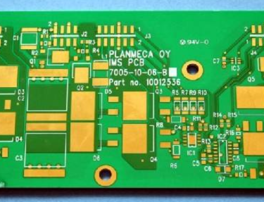
- Conductive Layers: The conductive layers are usually made of copper, which is laminated onto the substrate. Copper is chosen for its high electrical conductivity and ease of etching. The thickness of the copper layer can vary depending on the application, with common thicknesses ranging from 1 oz/ft² to 2 oz/ft².
- Solder Mask: The solder mask is a protective layer applied over the copper traces to prevent short circuits and oxidation. It is typically made of a polymer material and is available in various colors, with green being the most common.
- Silkscreen: The silkscreen layer is used to print labels, component identifiers, and other markings on the PCB. It is usually made of epoxy ink and is applied using a screen-printing process.
- Surface Finish: The surface finish is applied to the exposed copper areas to protect them from oxidation and improve solderability. Common surface finishes include HASL (Hot Air Solder Leveling), ENIG (Electroless Nickel Immersion Gold), and OSP (Organic Solderability Preservative).
The PCB Printing Process
The PCB printing process involves several steps, each of which must be executed with precision to ensure the final product meets the required specifications. The main steps in the PCB printing process are as follows:
- Design and Layout: The first step in PCB printing is designing the circuit layout using CAD software. The design includes the placement of components, routing of traces, and creation of vias (connections between layers). The design must adhere to specific design rules to ensure manufacturability and reliability.
- Printing the Circuit Pattern: Once the design is finalized, the circuit pattern is printed onto the substrate. This is typically done using a photolithographic process. A photosensitive layer, known as photoresist, is applied to the copper-clad substrate. The circuit pattern is then transferred onto the photoresist using a photomask and UV light. The exposed areas of the photoresist are then developed, leaving behind the desired circuit pattern.
- Etching: The next step is etching, where the unwanted copper is removed from the substrate. The board is immersed in an etching solution, such as ferric chloride or ammonium persulfate, which dissolves the exposed copper, leaving only the desired traces.
- Drilling: Holes are drilled into the PCB to accommodate through-hole components and vias. The drilling process is typically done using automated CNC (Computer Numerical Control) machines to ensure precision.
- Plating: After drilling, the holes are plated with copper to create electrical connections between layers. This is done using an electroplating process, where the board is immersed in a copper sulfate solution and an electric current is applied.
- Solder Mask Application: The solder mask is applied to the board to protect the copper traces and prevent short circuits. The solder mask is typically applied using a screen-printing process and then cured using UV light.
- Silkscreen Printing: The silkscreen layer is printed onto the board to add labels, component identifiers, and other markings. This is done using a screen-printing process with epoxy ink.
- Surface Finish: The final step in the PCB printing process is applying the surface finish to the exposed copper areas. This is done to protect the copper from oxidation and improve solderability. The surface finish is applied using various methods, depending on the type of finish being used.
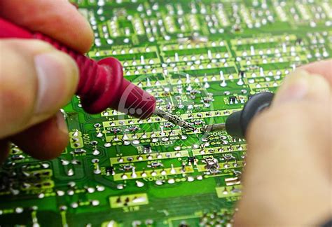
- Testing and Inspection: Once the PCB is fabricated, it undergoes rigorous testing and inspection to ensure it meets the required specifications. This includes electrical testing, visual inspection, and automated optical inspection (AOI) to detect any defects or errors.
Advancements in PCB Printing Technology
The field of PCB printing has seen significant advancements in recent years, driven by the demand for smaller, faster, and more complex electronic devices. Some of the key advancements include:
- High-Density Interconnect (HDI) PCBs: HDI PCBs are designed to accommodate a higher number of components in a smaller area. This is achieved by using finer traces, smaller vias, and multiple layers. HDI PCBs are commonly used in smartphones, tablets, and other compact electronic devices.
- Flexible and Rigid-Flex PCBs: Flexible PCBs are made from flexible materials like polyimide, allowing them to bend and conform to different shapes. Rigid-flex PCBs combine rigid and flexible sections, offering the benefits of both types. These PCBs are used in applications where space and weight are critical, such as wearable devices and aerospace systems.
- 3D Printing of PCBs: 3D printing technology is being explored for PCB fabrication, offering the potential for rapid prototyping and customization. 3D-printed PCBs can be created with complex geometries and integrated components, opening up new possibilities for design and functionality.
- Advanced Materials: New materials are being developed to improve the performance and reliability of PCBs. For example, low-loss dielectric materials are being used to reduce signal loss in high-frequency applications. Conductive inks and adhesives are also being developed for use in flexible and printed electronics.
- Automation and AI: Automation and artificial intelligence (AI) are being increasingly used in PCB manufacturing to improve efficiency and reduce errors. Automated optical inspection (AOI) systems use AI algorithms to detect defects and ensure quality control. AI is also being used to optimize PCB designs and manufacturing processes.
Challenges in PCB Printing
Despite the advancements in PCB printing technology, there are several challenges that manufacturers face:
- Miniaturization: As electronic devices become smaller and more complex, the demand for miniaturized PCBs with finer traces and smaller vias increases. This poses challenges in terms of precision and reliability.
- Signal Integrity: High-speed and high-frequency applications require PCBs with excellent signal integrity. This involves minimizing signal loss, crosstalk, and electromagnetic interference (EMI).
- Thermal Management: As electronic devices become more powerful, managing heat dissipation becomes a critical issue. PCBs must be designed to handle high temperatures and ensure efficient thermal management.
- Environmental Concerns: The PCB manufacturing process involves the use of hazardous chemicals and generates waste. There is a growing demand for environmentally friendly materials and processes to reduce the environmental impact of PCB production.
Conclusion
PCB printing is a complex and highly specialized process that plays a crucial role in the production of modern electronic devices. The field has evolved significantly over the years, driven by advancements in materials, technology, and manufacturing processes. Despite the challenges, the future of PCB printing looks promising, with ongoing research and development aimed at improving performance, reliability, and sustainability. As electronic devices continue to evolve, so too will the technology and techniques used in PCB printing, ensuring that PCBs remain at the heart of innovation in the electronics industry.


