Printed Circuit Boards (PCBs): The Backbone of Modern Electronics
Introduction
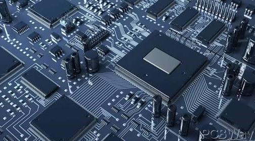
Printed Circuit Boards (PCBs) are the foundation of nearly all modern electronic devices. From smartphones and laptops to medical equipment and aerospace systems, PCBs provide the necessary electrical connections between components in a compact and efficient manner. Their design, manufacturing, and functionality have evolved significantly since their inception, enabling the rapid advancement of technology. This article explores the history, types, manufacturing processes, applications, and future trends of PCBs.
1. History of PCBs
The concept of PCBs dates back to the early 20th century. Before their invention, electronic circuits were assembled using point-to-point wiring, which was time-consuming, bulky, and prone to errors.
- Early Developments (1920s-1940s):
- In 1925, Charles Ducas patented a method for creating an electrical path directly on an insulated surface, laying the groundwork for PCBs.
- During World War II, the U.S. military used PCBs in proximity fuses for artillery shells, significantly improving reliability.
- Post-War Advancements (1950s-1970s):
- The invention of through-hole technology (THT) allowed components to be inserted into drilled holes and soldered onto the board.
- The introduction of fiberglass substrates (FR-4) improved durability and heat resistance.
- Modern Era (1980s-Present):
- Surface-mount technology (SMT) replaced through-hole in many applications, allowing for smaller and more densely packed PCBs.
- High-density interconnect (HDI) and flexible PCBs enabled new applications in wearables and IoT devices.
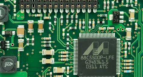
2. Types of PCBs
PCBs come in various forms, each suited for specific applications:
A. Based on Layers
- Single-Sided PCBs
- Conducting material on one side only.
- Used in simple electronics like calculators and LED lights.
- Double-Sided PCBs
- Conductive layers on both sides, connected by vias.
- Common in automotive dashboards and power supplies.
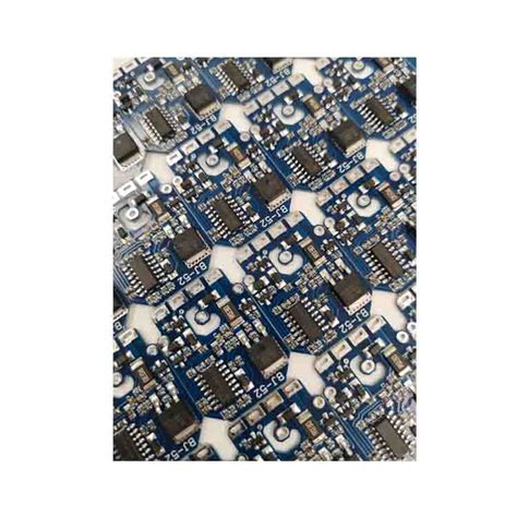
- Multi-Layer PCBs (4+ Layers)
- Used in complex devices like smartphones and servers.
- Enables high-speed signal transmission with reduced interference.
B. Based on Flexibility
- Rigid PCBs
- Made from solid materials like FR-4.
- Found in computers and industrial machinery.
- Flexible PCBs
- Made from polyimide or other flexible materials.
- Used in wearable devices and foldable smartphones.
- Rigid-Flex PCBs
- Combines rigid and flexible sections.
- Common in aerospace and medical implants.
C. Specialized PCBs
- High-Frequency PCBs – Used in RF and microwave applications.
- HDI PCBs – Enable ultra-miniaturization in modern electronics.
- Metal-Core PCBs – Improve heat dissipation in LED lighting.
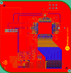
3. PCB Manufacturing Process
The production of PCBs involves several critical steps:
Step 1: Design & Layout
- Engineers use CAD software (e.g., Altium, Eagle) to design the circuit.
- Design rules check (DRC) ensures manufacturability.
Step 2: Printing the Circuit
- A photoresist layer is applied to a copper-clad board.
- UV light exposes the circuit pattern, and etching removes excess copper.
Step 3: Drilling & Plating
- Holes are drilled for through-hole components and vias.
- Electroless copper plating creates conductive pathways.
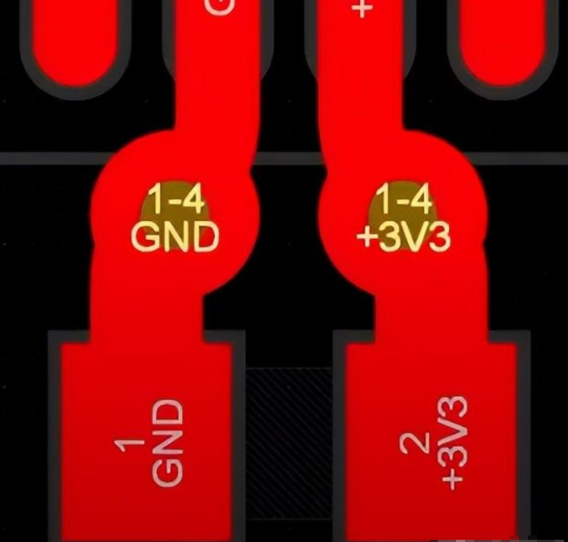
Step 4: Solder Mask & Silkscreen
- A solder mask (usually green) prevents short circuits.
- Silkscreen adds labels for component placement.
Step 5: Assembly (SMT & THT)
- Surface-Mount Technology (SMT):
- Components are placed and soldered using reflow ovens.
- Through-Hole Technology (THT):
- Components are inserted and wave-soldered.
Step 6: Testing & Quality Control
- Automated optical inspection (AOI) checks for defects.
- Electrical testing ensures functionality.
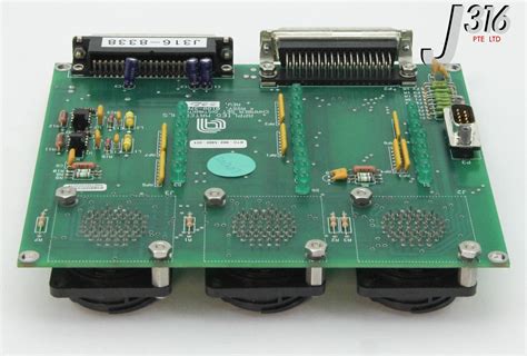
4. Applications of PCBs
PCBs are ubiquitous in modern technology:
- Consumer Electronics: Smartphones, laptops, TVs.
- Medical Devices: Pacemakers, MRI machines.
- Automotive Industry: Engine control units, infotainment systems.
- Aerospace & Defense: Avionics, radar systems.
- Industrial Automation: Robotics, control systems.
5. Future Trends in PCB Technology
- Miniaturization & Higher Density
- Advancements in HDI and microvia technology allow for smaller, more powerful devices.
- Flexible & Stretchable PCBs
- Growth in wearables and foldable electronics.
- Embedded Components
- Passive components (resistors, capacitors) embedded within the PCB to save space.
- 3D Printed Electronics
- Additive manufacturing could revolutionize rapid prototyping.
- Sustainable PCBs
- Biodegradable substrates and lead-free soldering for eco-friendly electronics.
Conclusion
PCBs are the unsung heroes of the digital age, enabling the seamless operation of countless electronic devices. As technology continues to evolve, so too will PCB design and manufacturing techniques, paving the way for even more innovative applications. Whether in consumer gadgets, medical breakthroughs, or space exploration, PCBs will remain at the heart of electronic advancement for decades to come.