Prototype pcb layout
Best Practices For Prototype PCB Layout Design
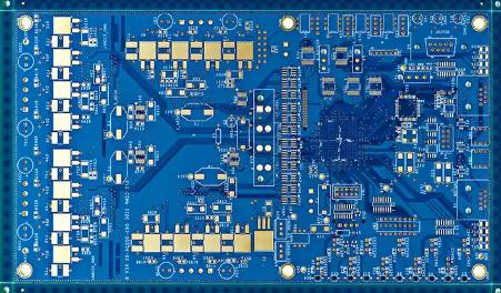
Designing a prototype printed circuit board (PCB) is a critical step in the development of electronic devices. It requires meticulous attention to detail and adherence to best practices to ensure functionality, reliability, and manufacturability.
One of the foremost considerations in prototype PCB layout design is the schematic capture.
This initial phase involves creating a detailed and accurate schematic diagram that serves as the blueprint for the PCB. Ensuring that the schematic is error-free is paramount, as any mistakes at this stage can propagate through to the final product, leading to costly revisions.
Transitioning from schematic capture to layout design, component placement becomes the next crucial step.
Strategic placement of components can significantly impact the performance and manufacturability of the PCB. It is advisable to place components in a logical order, grouping related components together to minimize signal path lengths and reduce potential interference. Additionally, placing components with similar functions in close proximity can simplify routing and improve signal integrity.
Once components are placed, the routing of electrical connections, or traces, must be carefully planned.
Effective routing is essential for maintaining signal integrity and ensuring that the PCB functions as intended. It is important to follow design rules and guidelines, such as maintaining appropriate trace widths and spacing to handle the required current and voltage levels. Furthermore, using a ground plane can help reduce electromagnetic interference (EMI) and provide a stable reference for signal return paths.
In addition to routing, attention must be given to power distribution.
Ensuring that power and ground planes are properly designed can prevent issues such as voltage drops and noise. Utilizing decoupling capacitors near power pins of integrated circuits can help filter out noise and provide a stable power supply. Moreover, it is beneficial to use multiple vias to connect power and ground planes, which can reduce inductance and improve current carrying capacity.
Thermal management is another critical aspect of prototype PCB layout design.
Components that generate significant heat, such as power transistors and voltage regulators, should be placed in areas with adequate airflow or near heat sinks. Additionally, using thermal vias and copper pours can help dissipate heat more effectively, preventing overheating and ensuring the longevity of the components.
Design for manufacturability (DFM) is an essential consideration throughout the PCB layout process.
Ensuring that the design adheres to the capabilities and limitations of the chosen manufacturing process can prevent issues during production. This includes adhering to minimum trace widths, spacing, and hole sizes, as well as considering the placement of test points for easier testing and debugging.
Finally, thorough design reviews and simulations are indispensable before moving to the fabrication stage.
Conducting design rule checks (DRC) and electrical rule checks (ERC) can help identify potential issues that may have been overlooked. Additionally, using simulation tools to analyze signal integrity, power integrity, and thermal performance can provide valuable insights and help optimize the design.
In conclusion, following best practices for prototype PCB layout design is essential for creating a functional, reliable, and manufacturable product. From schematic capture and component placement to routing, power distribution, thermal management, and design for manufacturability, each step requires careful consideration and attention to detail. By adhering to these best practices and conducting thorough reviews and simulations, designers can significantly increase the likelihood of success in their prototype PCB projects.
Common Mistakes To Avoid In Prototype PCB Layout
When designing a prototype PCB layout, it is crucial to be aware of common mistakes that can compromise the functionality and reliability of the final product. One of the most frequent errors is neglecting to consider the electrical noise and interference that can arise from improper component placement. Ensuring that high-frequency components are adequately isolated from sensitive analog circuits can mitigate this issue. Additionally, placing decoupling capacitors close to the power pins of integrated circuits can help filter out noise and stabilize the power supply.
Another common mistake is failing to adhere to design for manufacturability (DFM) guidelines.
Overlooking these guidelines can result in a PCB that is difficult or even impossible to manufacture. For instance, using trace widths that are too narrow or spacing components too closely together can lead to production issues. It is essential to consult with your PCB manufacturer early in the design process to understand their specific capabilities and limitations, thereby avoiding costly redesigns and delays.
Thermal management is another critical aspect that is often underestimated in prototype PCB layouts.
Components that generate significant heat, such as power transistors and voltage regulators, need to be placed in a manner that allows for efficient heat dissipation. Failing to do so can lead to overheating and potential failure of the PCB. Utilizing thermal vias, heat sinks, and proper airflow can help manage heat effectively.
Signal integrity is another area where designers frequently make mistakes.
Poor signal routing can lead to issues such as crosstalk, signal reflection, and electromagnetic interference (EMI). To avoid these problems, it is important to maintain consistent trace impedance and use proper grounding techniques. Differential pairs should be routed together with controlled spacing, and signal traces should be kept as short as possible to minimize delay and distortion.
Grounding issues are also a common pitfall in prototype PCB layouts.
A poor grounding scheme can result in ground loops, which can introduce noise and affect the performance of the circuit. Implementing a solid ground plane and ensuring that all components have a low-impedance path to ground can help mitigate these issues. Additionally, separating analog and digital grounds and connecting them at a single point can further improve performance.
Component selection and placement are other areas where mistakes are often made.
Choosing components that are not readily available or have long lead times can delay the entire project. It is advisable to select components that are in stock and have multiple sources to ensure availability. Furthermore, placing components without considering their orientation and accessibility for testing and debugging can complicate the prototyping phase. Ensuring that test points are accessible and that components are oriented for easy probing can facilitate troubleshooting.
Lastly, documentation is an often-overlooked aspect of prototype PCB layout.
Incomplete or inaccurate documentation can lead to misunderstandings and errors during manufacturing and assembly. Providing detailed schematics, bill of materials (BOM), and assembly drawings can help ensure that the PCB is built correctly and functions as intended.
In conclusion, avoiding these common mistakes in prototype PCB layout requires careful planning and attention to detail. By considering factors such as electrical noise, manufacturability, thermal management, signal integrity, grounding, component selection, and documentation, designers can create more reliable and functional PCBs. Taking the time to address these issues during the design phase can save significant time and resources in the long run, ultimately leading to a successful prototype.

Tools And Software For Efficient Prototype PCB Layout
In the realm of electronics design, the creation of a prototype printed circuit board (PCB) is a critical step that bridges the gap between conceptualization and mass production. To achieve an efficient prototype PCB layout, engineers and designers rely on a variety of tools and software that streamline the design process, enhance accuracy, and ensure the functionality of the final product. These tools and software are indispensable in managing the complexities of modern PCB design, from schematic capture to layout and verification.
One of the foundational tools in PCB design is schematic capture software.
This software allows designers to create a detailed diagram of the electronic circuit, specifying the components and their interconnections. Popular schematic capture tools such as Altium Designer, Eagle, and KiCad provide robust features that facilitate the organization and documentation of the circuit design.
These tools often include extensive libraries of electronic components, which can be easily integrated into the schematic, thereby reducing the time and effort required to create a comprehensive design.
Transitioning from schematic capture to PCB layout, designers utilize layout software to translate the schematic into a physical board design.
This software enables the placement of components on the PCB and the routing of electrical connections between them. Altium Designer, for instance, offers advanced layout capabilities, including 3D visualization, which allows designers to view the PCB from different angles and ensure that components are correctly placed and aligned. Similarly, Eagle provides a user-friendly interface and powerful routing tools that help in creating efficient and compact PCB layouts. KiCad, an open-source alternative, is also widely used due to its flexibility and cost-effectiveness.
In addition to schematic capture and layout tools, simulation software plays a crucial role in the PCB design process.
Simulation tools such as SPICE (Simulation Program with Integrated Circuit Emphasis) allow designers to test the behavior of their circuits before committing to a physical prototype. By simulating the electrical performance of the circuit, designers can identify and rectify potential issues, such as signal integrity problems or power distribution challenges, early in the design process. This preemptive approach not only saves time but also reduces the likelihood of costly errors in the final prototype.
Moreover, design rule checking (DRC) and electrical rule checking (ERC) are essential features integrated into most PCB design software.
These tools automatically verify that the design adheres to predefined rules and standards, ensuring that the PCB can be manufactured without issues. DRC checks for violations related to component placement, trace widths, and spacing, while ERC focuses on electrical constraints, such as proper grounding and signal routing. By leveraging these automated checks, designers can maintain high standards of quality and reliability in their PCB layouts.
Furthermore, collaboration and version control tools are increasingly important in modern PCB design workflows.
Platforms like Git and cloud-based design environments enable multiple designers to work on the same project simultaneously, track changes, and manage different versions of the design. This collaborative approach enhances productivity and ensures that all team members are aligned throughout the design process.
In conclusion, the efficient layout of prototype PCBs is facilitated by a suite of specialized tools and software that address various aspects of the design process. From schematic capture and layout to simulation and rule checking, these tools provide the necessary capabilities to create accurate and reliable PCB prototypes. As technology continues to evolve, the integration of advanced features and collaborative platforms will further enhance the efficiency and effectiveness of PCB design, ultimately leading to better electronic products.
Step-By-Step Guide To Creating A Prototype PCB Layout
Creating a prototype PCB layout is a critical step in the development of electronic devices, serving as the blueprint for the final product. The process involves several meticulous steps, each requiring careful attention to detail to ensure the functionality and reliability of the circuit. To begin with, it is essential to have a clear understanding of the circuit design and the components involved. This initial phase involves creating a schematic diagram, which serves as a visual representation of the electrical connections and components. The schematic diagram is the foundation upon which the PCB layout is built, and it is crucial to ensure its accuracy before proceeding.
Once the schematic is finalized, the next step is to select the appropriate PCB design software.
There are various software options available, each offering different features and capabilities. Popular choices include Altium Designer, Eagle, and KiCad. The selection of software depends on factors such as the complexity of the design, budget, and personal preference. After choosing the software, the schematic diagram is imported into the PCB layout environment, where the actual design process begins.
The placement of components on the PCB is a critical aspect of the layout process.
Components should be arranged in a manner that minimizes signal interference and optimizes the overall performance of the circuit. It is advisable to place components with similar functions close to each other and to consider the flow of signals through the circuit. Additionally, attention should be given to the placement of power and ground planes, as these are essential for the stability and performance of the circuit.
Following the placement of components, the next step is to route the electrical connections, or traces, between them.
This process involves drawing lines on the PCB to connect the various pins of the components according to the schematic diagram. It is important to follow best practices for trace routing, such as keeping traces as short as possible, avoiding sharp angles, and maintaining adequate spacing between traces to prevent short circuits and signal interference. In some cases, it may be necessary to use multiple layers for routing, especially for complex designs with a high density of components.
After completing the routing, it is essential to perform a thorough design rule check (DRC) to ensure that the layout adheres to the manufacturing constraints and industry standards. The DRC process involves checking for issues such as minimum trace width, spacing violations, and clearance between components. Any errors identified during this check must be addressed before proceeding to the next step.
Once the design rule check is complete, the final step is to generate the necessary files for manufacturing the PCB.
These files, commonly referred to as Gerber files, contain all the information required by the PCB manufacturer to produce the board. It is important to review these files carefully to ensure that they accurately represent the intended design. Additionally, it may be beneficial to create a bill of materials (BOM) that lists all the components required for the assembly of the PCB.
In conclusion, creating a prototype PCB layout involves a series of methodical steps, each requiring careful consideration and attention to detail. From the initial schematic design to the final generation of manufacturing files, each phase plays a crucial role in ensuring the success of the final product. By following best practices and utilizing appropriate tools, designers can create reliable and efficient PCB layouts that meet the desired specifications and performance criteria.