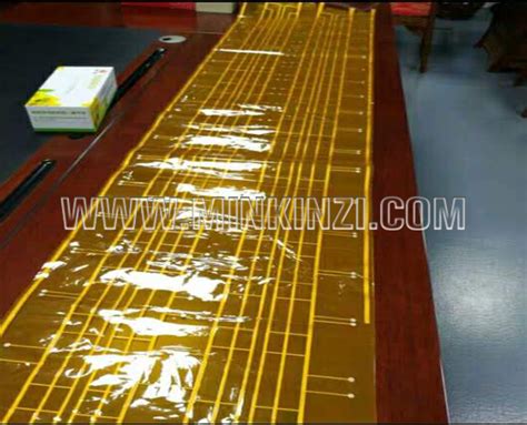
Prototype pcb tracks
Designing Efficient Prototype PCB Tracks
Designing efficient prototype PCB tracks is a critical aspect of electronic circuit development, requiring meticulous attention to detail and a comprehensive understanding of both theoretical and practical considerations.
The process begins with a clear schematic, which serves as the blueprint for the physical layout of the printed circuit board (PCB). Translating this schematic into an effective PCB design necessitates a careful balance between electrical performance, manufacturability, and reliability.
One of the primary considerations in designing PCB tracks is the width of the traces.
The width must be sufficient to carry the required current without excessive heating, which can lead to performance degradation or even failure. The IPC-2221 standard provides guidelines for determining appropriate trace widths based on current-carrying capacity and temperature rise. Additionally, the choice of copper thickness, typically measured in ounces per square foot, plays a significant role in defining the trace width. Thicker copper layers can carry more current, allowing for narrower traces, which can be beneficial in high-density designs.
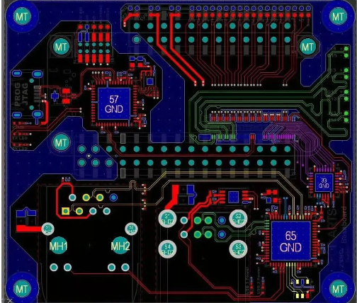
Another crucial factor is the layout of the tracks themselves.
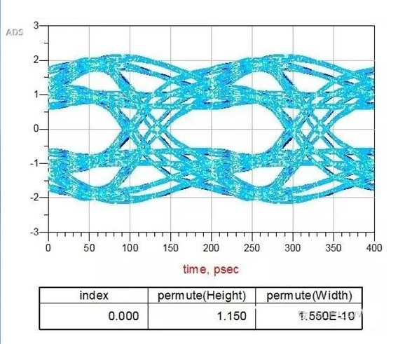
Signal integrity is paramount, especially in high-speed digital circuits where issues such as crosstalk, electromagnetic interference (EMI), and signal reflection can severely impact performance. To mitigate these issues, designers often employ techniques such as controlled impedance routing, differential pair routing, and proper grounding practices. Controlled impedance routing ensures that the characteristic impedance of a trace remains consistent, which is vital for maintaining signal integrity. Differential pair routing, on the other hand, involves routing two complementary signals together to reduce noise and improve signal quality.
Grounding is another essential aspect of PCB track design.
A well-designed ground plane can significantly reduce EMI and provide a stable reference voltage for the entire circuit. It is crucial to minimize the number of breaks in the ground plane and to ensure that all components have a low-impedance path to ground. Additionally, the placement of decoupling capacitors near power pins can help filter out noise and stabilize the power supply.
Thermal management is also a key consideration in PCB design.
Components that generate significant heat, such as power transistors or voltage regulators, require adequate cooling to maintain their performance and longevity. This can be achieved through the use of thermal vias, heat sinks, and careful placement of components to ensure efficient heat dissipation. Thermal vias are small holes filled with conductive material that help transfer heat from the top layer of the PCB to the bottom layer, where it can be dissipated more effectively.
Furthermore, manufacturability must be taken into account during the design process.
This includes ensuring that the PCB can be produced using standard fabrication processes and that it meets the tolerances and capabilities of the chosen manufacturer. Design for manufacturability (DFM) guidelines suggest maintaining adequate spacing between traces, pads, and vias to prevent short circuits and ensure reliable soldering. Additionally, incorporating test points and designing for ease of assembly can streamline the production process and reduce costs.
In conclusion, designing efficient prototype PCB tracks involves a delicate balance of multiple factors, including trace width, signal integrity, grounding, thermal management, and manufacturability. By carefully considering each of these elements and employing best practices, designers can create robust and reliable PCBs that meet the demands of modern electronic applications. The integration of these principles not only enhances the performance and reliability of the final product but also ensures a smoother transition from prototype to production.
Common Mistakes in Prototype PCB Track Layout
When designing prototype printed circuit boards (PCBs), engineers and designers often encounter a variety of challenges that can lead to common mistakes in track layout. These errors, if not addressed, can significantly impact the functionality, reliability, and manufacturability of the final product. One prevalent mistake is the improper management of track width and spacing. Ensuring that tracks are neither too narrow nor too close to each other is crucial for maintaining signal integrity and preventing short circuits. Narrow tracks can lead to increased resistance and potential overheating, while insufficient spacing can result in electrical shorts, especially in high-voltage applications.
Another frequent issue is the inadequate consideration of return paths for high-frequency signals.
High-frequency signals require a clear and direct return path to minimize electromagnetic interference (EMI) and signal degradation. Failing to provide a proper return path can lead to increased noise and reduced performance of the PCB. To mitigate this, designers should ensure that ground planes are continuous and that signal tracks are routed in close proximity to their corresponding ground paths.
Thermal management is another critical aspect that is often overlooked in prototype PCB track layout.
Components that generate significant heat need to be placed strategically to ensure efficient heat dissipation. Tracks should be designed to facilitate the flow of heat away from sensitive components. Additionally, the use of thermal vias and heat sinks can help manage heat distribution across the PCB. Neglecting thermal considerations can lead to overheating, which can damage components and reduce the overall lifespan of the PCB.
Furthermore, the placement of decoupling capacitors is a common area where mistakes are made.
Decoupling capacitors are essential for filtering out noise and stabilizing power supply voltages. They should be placed as close as possible to the power pins of integrated circuits (ICs) to be effective. Placing them too far away can reduce their effectiveness and lead to power supply instability. Designers should also ensure that the tracks connecting decoupling capacitors to the ICs are short and have low inductance.
Another common mistake is the failure to consider the manufacturability of the PCB.
Designers should be aware of the capabilities and limitations of the PCB fabrication process. For instance, extremely fine pitch components and very narrow tracks may be difficult to manufacture reliably. It is essential to adhere to the design rules provided by the PCB manufacturer to ensure that the prototype can be produced without issues. Additionally, incorporating test points and considering the ease of assembly can facilitate troubleshooting and testing during the prototyping phase.
Signal integrity is another critical factor that can be compromised by poor track layout.
Crosstalk, which occurs when signals on adjacent tracks interfere with each other, can be a significant issue, particularly in high-speed designs. To minimize crosstalk, designers should maintain adequate spacing between high-speed signal tracks and use differential pairs where appropriate. Additionally, careful attention should be paid to the routing of clock signals and other critical paths to ensure minimal signal degradation.
In conclusion, avoiding common mistakes in prototype PCB track layout requires careful consideration of various factors, including track width and spacing, return paths for high-frequency signals, thermal management, placement of decoupling capacitors, manufacturability, and signal integrity. By addressing these aspects during the design phase, engineers can enhance the performance, reliability, and manufacturability of their PCBs, ultimately leading to more successful prototypes and final products.
Advanced Techniques for Prototype PCB Track Routing
When designing prototype printed circuit boards (PCBs), the routing of tracks is a critical aspect that can significantly influence the performance and reliability of the final product. Advanced techniques in PCB track routing are essential for ensuring signal integrity, minimizing electromagnetic interference (EMI), and optimizing the overall functionality of the circuit. To achieve these objectives, designers must employ a combination of strategic planning, sophisticated software tools, and a deep understanding of electrical principles.
One of the foremost considerations in advanced PCB track routing is the management of signal integrity.
High-speed signals, in particular, are susceptible to issues such as crosstalk, reflection, and signal degradation. To mitigate these problems, designers often use controlled impedance routing, which involves maintaining a consistent impedance along the length of a track. This can be achieved by carefully selecting the width of the track and the distance between the track and the reference plane. Additionally, differential pair routing is commonly employed for high-speed signals. By routing two complementary signals in parallel with a constant spacing, differential pairs can effectively reduce noise and improve signal integrity.
Another critical aspect of advanced PCB track routing is the minimization of electromagnetic interference (EMI).
EMI can be a significant concern, especially in densely packed PCBs with multiple high-frequency components. To address this, designers can use techniques such as ground planes and shielding. Ground planes provide a low-impedance path for return currents, which helps to reduce EMI. Shielding, on the other hand, involves enclosing sensitive tracks or components with conductive materials to block external electromagnetic fields. Additionally, careful placement of decoupling capacitors near power pins can help to filter out high-frequency noise and further reduce EMI.
Thermal management is also a crucial factor in advanced PCB track routing.
As electronic components become more powerful and compact, the heat generated by these components can pose a significant challenge. To ensure proper thermal management, designers can use techniques such as thermal vias and heat sinks. Thermal vias are small holes filled with conductive material that connect different layers of the PCB, allowing heat to dissipate more effectively. Heat sinks, which are attached to high-power components, can also help to dissipate heat and prevent overheating.
Furthermore, the use of advanced software tools has revolutionized the process of PCB track routing.
Modern PCB design software offers a range of features that can automate and optimize the routing process. For instance, auto-routing algorithms can quickly generate efficient routing paths based on predefined design rules. These tools can also perform signal integrity analysis, thermal analysis, and EMI simulation, allowing designers to identify and address potential issues early in the design process. By leveraging these advanced software tools, designers can significantly reduce the time and effort required for PCB track routing while ensuring high-quality results.
In addition to these techniques, collaboration and communication among team members are essential for successful PCB track routing.
Complex PCB designs often involve multiple engineers working on different aspects of the project. Effective communication and collaboration tools can help to ensure that all team members are on the same page and that design changes are properly documented and implemented. This collaborative approach can help to prevent errors and ensure that the final PCB design meets all performance and reliability requirements.
In conclusion, advanced techniques for prototype PCB track routing are essential for achieving optimal performance and reliability in modern electronic devices. By focusing on signal integrity, minimizing EMI, managing thermal issues, leveraging advanced software tools, and fostering collaboration among team members, designers can create high-quality PCB designs that meet the demanding requirements of today’s technology.

Tools and Software for Prototype PCB Track Design
Designing prototype PCB tracks is a critical step in the development of electronic devices, requiring precision, accuracy, and the right set of tools and software. The process begins with conceptualizing the circuit design, which is then translated into a physical layout on a printed circuit board (PCB). To achieve this, engineers and designers rely on a variety of tools and software that facilitate the creation, simulation, and testing of PCB tracks.
One of the primary tools used in prototype PCB track design is Electronic Design Automation (EDA) software.
EDA tools provide a comprehensive suite of functionalities that include schematic capture, layout design, and simulation. Among the most popular EDA tools are Altium Designer, Eagle, and KiCad. Altium Designer is renowned for its advanced features and user-friendly interface, making it a preferred choice for professional designers. Eagle, on the other hand, is favored for its extensive library of components and ease of use, while KiCad is an open-source alternative that offers robust capabilities without the associated costs.
Transitioning from schematic capture to layout design, these tools enable designers to place components and route electrical connections with precision.
The layout design phase involves defining the physical dimensions of the PCB, placing components in optimal positions, and routing the tracks that connect these components. This step is crucial as it directly impacts the performance and reliability of the final product. EDA tools provide various routing options, including manual routing, auto-routing, and differential pair routing, each catering to different design requirements and complexities.
Simulation is another vital aspect of prototype PCB track design.
Before committing to the physical production of a PCB, it is essential to simulate the circuit to identify potential issues such as signal integrity problems, electromagnetic interference, and thermal management concerns. Tools like SPICE (Simulation Program with Integrated Circuit Emphasis) are commonly used for this purpose. SPICE allows designers to simulate the behavior of their circuits under different conditions, providing valuable insights that can be used to refine the design.
In addition to EDA tools, designers often use specialized software for specific tasks.
For instance, Gerber file viewers are essential for inspecting the final output files that will be sent to PCB manufacturers. These viewers allow designers to verify that the PCB layout meets all design specifications and manufacturing requirements. Furthermore, Design Rule Check (DRC) and Electrical Rule Check (ERC) tools are employed to ensure that the design adheres to predefined rules and standards, minimizing the risk of errors during production.
Collaboration and version control are also important considerations in prototype PCB track design.
Tools like Git and SVN (Subversion) are commonly used to manage changes and maintain a history of design iterations. These tools facilitate collaboration among team members, allowing multiple designers to work on the same project simultaneously while keeping track of modifications and updates.
In conclusion, the design of prototype PCB tracks is a multifaceted process that relies heavily on a suite of specialized tools and software. From EDA tools for schematic capture and layout design to simulation software and Gerber file viewers, each tool plays a crucial role in ensuring the accuracy and reliability of the final product. By leveraging these tools effectively, designers can streamline the development process, reduce the likelihood of errors, and ultimately produce high-quality PCBs that meet the desired specifications.