Quality control in pcb manufacturing
Importance Of Quality Control In PCB Manufacturing
Quality control in PCB manufacturing is a critical aspect that ensures the reliability and functionality of electronic devices. The importance of quality control cannot be overstated, as it directly impacts the performance, safety, and longevity of the final product. In the highly competitive electronics industry, maintaining stringent quality control measures is essential for manufacturers to meet industry standards and customer expectations.
To begin with, quality control in PCB manufacturing involves a series of systematic procedures designed to detect and rectify defects at various stages of production.
This process starts with the inspection of raw materials, such as copper-clad laminates and solder masks, to ensure they meet the required specifications. By verifying the quality of these materials before they enter the production line, manufacturers can prevent potential issues that may arise later in the process.
As the manufacturing process progresses, quality control measures become even more critical.
During the fabrication stage, PCBs undergo various processes such as drilling, plating, and etching. Each of these steps must be meticulously monitored to ensure precision and accuracy. For instance, the drilling process must be executed with exacting standards to avoid misalignment, which can lead to connectivity issues in the final product. Similarly, the plating process must ensure uniform deposition of conductive materials to maintain electrical integrity.
Moreover, the assembly stage of PCB manufacturing is another crucial point where quality control plays a vital role.
Components must be accurately placed and soldered onto the PCB to ensure proper functionality. Automated optical inspection (AOI) and X-ray inspection are commonly employed techniques to detect any misalignments, soldering defects, or component placement errors. These advanced inspection methods enable manufacturers to identify and address issues promptly, thereby reducing the likelihood of defective products reaching the market.
In addition to these inspection techniques, functional testing is an integral part of quality control in PCB manufacturing.
This involves subjecting the assembled PCBs to various electrical tests to verify their performance under different conditions. Functional testing helps identify any potential issues related to signal integrity, power distribution, and thermal management. By conducting these tests, manufacturers can ensure that the PCBs meet the required performance standards and are capable of operating reliably in their intended applications.
Furthermore, quality control in PCB manufacturing extends beyond the production process to include environmental and regulatory compliance.
Manufacturers must adhere to industry standards such as IPC (Institute for Printed Circuits) and RoHS (Restriction of Hazardous Substances) to ensure their products are safe and environmentally friendly. Compliance with these standards not only enhances the credibility of the manufacturer but also ensures that the PCBs are free from harmful substances and meet global safety requirements.
In conclusion, the importance of quality control in PCB manufacturing cannot be emphasized enough. It is a multifaceted process that encompasses the inspection of raw materials, monitoring of fabrication and assembly stages, and rigorous functional testing. By implementing stringent quality control measures, manufacturers can ensure the production of reliable, high-performance PCBs that meet industry standards and customer expectations. This, in turn, enhances the overall quality and safety of electronic devices, thereby contributing to the advancement of technology and innovation in the electronics industry.

Key Quality Control Techniques For PCB Production
Quality control in PCB manufacturing is a critical aspect that ensures the reliability and functionality of printed circuit boards. The process involves a series of meticulous techniques designed to detect and rectify defects at various stages of production. One of the primary techniques employed is visual inspection, which serves as the first line of defense against potential flaws. Technicians use magnification tools to scrutinize the boards for visible defects such as misaligned components, solder bridges, and surface irregularities. This initial step is crucial as it helps identify issues that could compromise the board’s performance.
Following visual inspection, automated optical inspection (AOI) is often utilized to enhance accuracy.
AOI systems use high-resolution cameras and sophisticated algorithms to compare the manufactured PCB against a predefined template. This method is highly effective in detecting minute discrepancies that might be overlooked during manual inspection. By automating the process, AOI not only increases the speed of inspection but also reduces human error, thereby ensuring a higher level of precision.
In addition to AOI, X-ray inspection is another pivotal technique in quality control for PCB production.
This method is particularly useful for examining the internal structures of the board, such as solder joints and vias, which are not visible to the naked eye. X-ray inspection can reveal hidden defects like voids, cracks, and insufficient soldering, which could lead to electrical failures if left unaddressed. By providing a non-destructive means of inspection, X-ray technology allows manufacturers to maintain the integrity of the PCB while ensuring its quality.
Electrical testing is also an integral part of the quality control process.
This technique involves subjecting the PCB to various electrical tests to verify its functionality. One common method is the in-circuit test (ICT), which checks for shorts, opens, resistance, capacitance, and other electrical parameters. ICT is highly effective in identifying functional defects and ensuring that the PCB meets the required specifications. Another method, known as the flying probe test, uses moving probes to test the electrical performance of the board without the need for a custom fixture. This flexibility makes it ideal for small production runs and prototype testing.
Moreover, environmental stress screening (ESS) is employed to assess the durability of PCBs under extreme conditions.
This technique subjects the boards to thermal cycling, vibration, and other stress factors to simulate real-world operating environments. ESS helps identify potential weaknesses that could lead to premature failure, thereby ensuring that only robust and reliable PCBs reach the market.
Furthermore, solder paste inspection (SPI) is a specialized technique used to evaluate the quality of solder paste application.
SPI systems measure the volume, height, and alignment of solder paste deposits to ensure they meet the required standards. Proper solder paste application is crucial for achieving strong solder joints and preventing defects such as tombstoning and insufficient soldering.
In conclusion, quality control in PCB manufacturing encompasses a range of techniques designed to detect and rectify defects at various stages of production. From visual inspection and automated optical inspection to X-ray inspection and electrical testing, each method plays a vital role in ensuring the reliability and functionality of printed circuit boards. By employing these techniques, manufacturers can maintain high standards of quality, thereby enhancing the performance and longevity of their products.
Common Quality Control Challenges In PCB Manufacturing
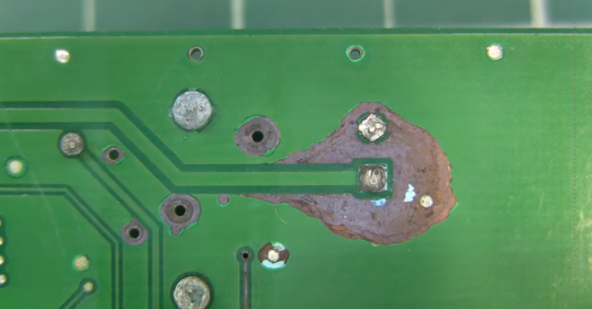
In the realm of printed circuit board (PCB) manufacturing, quality control is paramount to ensure the reliability and functionality of the final product. However, achieving consistent quality is fraught with numerous challenges that manufacturers must navigate. One of the most prevalent issues is the occurrence of defects during the fabrication process. These defects can range from minor cosmetic imperfections to critical faults that compromise the entire board’s performance. For instance, issues such as solder bridging, where solder forms an unintended connection between two points, can lead to short circuits and device failure. Similarly, open circuits, where a break in the conductive path occurs, can render the PCB non-functional.
Another significant challenge in PCB manufacturing is maintaining dimensional accuracy.
As PCBs become increasingly complex and miniaturized, the tolerances for errors become exceedingly tight. Even slight deviations in the dimensions of the board or the placement of components can lead to misalignment and connectivity issues. This is particularly problematic in high-density interconnect (HDI) boards, where the margin for error is minimal. Ensuring that each layer of the PCB aligns perfectly with the others requires meticulous attention to detail and precise control over the manufacturing process.
Furthermore, the materials used in PCB manufacturing can also pose quality control challenges.
The choice of substrate material, copper thickness, and solder mask can all impact the board’s performance and durability. For example, variations in the copper thickness can affect the board’s electrical properties, leading to inconsistent signal transmission. Additionally, the solder mask must be applied uniformly to prevent exposure of the underlying copper, which can lead to corrosion and reduced lifespan of the PCB. Ensuring consistency in material properties requires rigorous testing and quality assurance protocols.
Environmental factors also play a crucial role in PCB manufacturing quality control.
temperature and humidity levels in the manufacturing environment can significantly impact the soldering process and the adhesion of components to the board. Excessive humidity can lead to oxidation of the copper traces, while temperature fluctuations can cause thermal stress, leading to warping or delamination of the PCB layers. Maintaining a controlled environment is essential to mitigate these risks and ensure the integrity of the final product.
Moreover, the inspection and testing processes themselves can introduce challenges.
Automated optical inspection (AOI) and X-ray inspection are commonly used to detect defects and verify the quality of the PCB. However, these methods are not infallible and can sometimes miss subtle defects or generate false positives. Ensuring the accuracy and reliability of inspection equipment is critical to identifying and addressing quality issues before the boards are shipped to customers.
In addition to these technical challenges, there are also logistical and operational hurdles to consider.
The global nature of the electronics supply chain means that PCB manufacturers often source components and materials from multiple suppliers. Variability in the quality of these inputs can lead to inconsistencies in the final product. Establishing strong relationships with reliable suppliers and implementing stringent incoming quality control measures are essential to mitigate this risk.
In conclusion, quality control in PCB manufacturing is a multifaceted challenge that requires a comprehensive approach. From managing defects and maintaining dimensional accuracy to controlling environmental factors and ensuring reliable inspection processes, manufacturers must address a wide range of issues to produce high-quality PCBs. By implementing robust quality assurance protocols and continuously monitoring and improving their processes, manufacturers can overcome these challenges and deliver reliable, high-performance PCBs to their customers.

Role Of Automated Testing In PCB Quality Assurance
In the realm of printed circuit board (PCB) manufacturing, quality control is paramount to ensure the reliability and functionality of the final product. One of the most significant advancements in this field is the integration of automated testing systems, which play a crucial role in PCB quality assurance. These systems not only enhance the precision and efficiency of the testing process but also mitigate the risk of human error, thereby ensuring a higher standard of quality.
Automated testing in PCB manufacturing encompasses a variety of techniques and technologies designed to evaluate the integrity and performance of the boards.
Among these, Automated Optical Inspection (AOI) and Automated X-ray Inspection (AXI) are particularly noteworthy. AOI utilizes high-resolution cameras and sophisticated algorithms to detect surface defects such as soldering issues, component misalignments, and other anomalies. By providing real-time feedback, AOI systems enable manufacturers to promptly address any defects, thus preventing faulty boards from progressing further along the production line.
Similarly, AXI offers a non-destructive means of inspecting the internal structures of PCBs.
This technology is especially valuable for identifying hidden defects such as voids, cracks, and insufficient solder joints that are not visible to the naked eye. By employing X-ray imaging, AXI systems can penetrate the layers of the PCB, offering a comprehensive view of its internal composition. This level of scrutiny is essential for ensuring the structural integrity and long-term reliability of the boards, particularly in applications where failure is not an option.
Transitioning from inspection to functional testing, In-Circuit Testing (ICT) and Flying Probe Testing (FPT) are integral components of automated PCB quality assurance.
ICT involves the use of fixed probes to test the electrical performance of individual components on the board. This method is highly effective for verifying the functionality of complex circuits and identifying issues such as short circuits, open circuits, and incorrect component values. On the other hand, FPT employs movable probes to test the electrical characteristics of the PCB without the need for custom fixtures. This flexibility makes FPT particularly suitable for low-volume production runs and prototype testing, where rapid turnaround and adaptability are crucial.
Moreover, the integration of automated testing systems into the PCB manufacturing process offers several ancillary benefits.
For instance, the data collected during automated testing can be leveraged for statistical process control (SPC), enabling manufacturers to identify trends and patterns that may indicate underlying issues in the production process. By analyzing this data, manufacturers can implement corrective actions to address root causes, thereby enhancing overall process efficiency and product quality.
Furthermore, automated testing systems contribute to cost savings by reducing the need for manual inspection and rework.
The precision and consistency of automated systems minimize the likelihood of defects, which in turn reduces the incidence of costly recalls and warranty claims. Additionally, the speed and accuracy of automated testing facilitate faster production cycles, enabling manufacturers to meet tight deadlines and respond swiftly to market demands.
In conclusion, the role of automated testing in PCB quality assurance cannot be overstated. By incorporating advanced inspection and testing technologies, manufacturers can achieve a higher level of precision, efficiency, and reliability in their production processes. These systems not only enhance the quality of the final product but also offer significant cost savings and operational benefits. As the demand for high-performance PCBs continues to grow, the adoption of automated testing will undoubtedly remain a cornerstone of quality control in the industry.