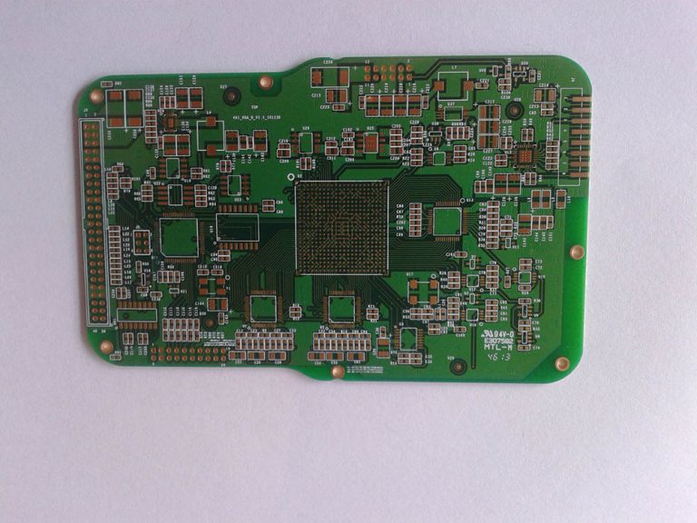
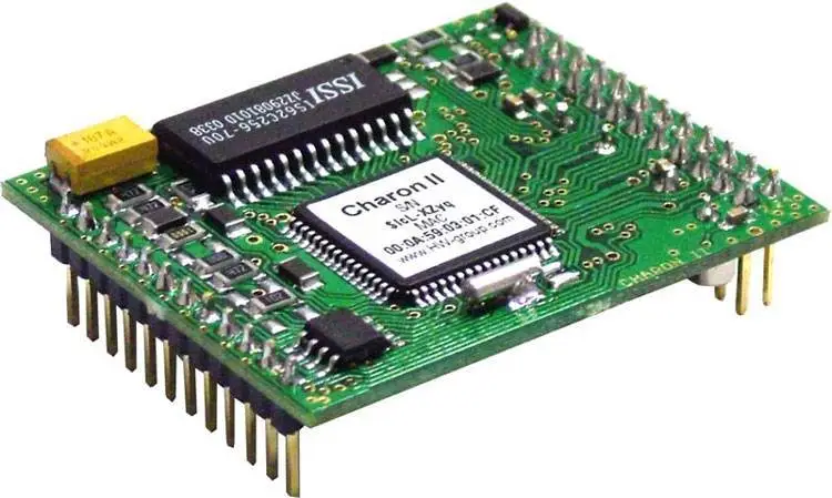
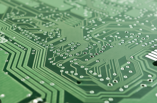
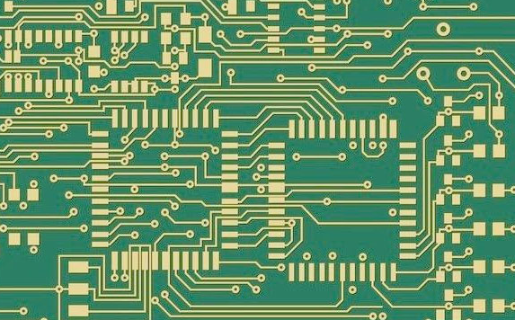
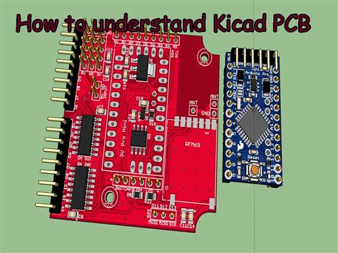
Rapid pcb prototype
Advances In Rapid PCB Prototype Technologies
The field of rapid PCB (Printed Circuit Board) prototyping has witnessed significant advancements in recent years, driven by the increasing demand for faster, more efficient, and cost-effective methods of producing electronic circuits. These advancements have been propelled by innovations in materials, manufacturing processes, and design software, which collectively contribute to the acceleration of PCB development cycles.
One of the most notable advancements in rapid PCB prototyping is the development of additive manufacturing techniques, commonly known as 3D printing.
Unlike traditional subtractive methods, which involve removing material to create the desired circuit pattern, additive manufacturing builds the PCB layer by layer. This approach not only reduces material waste but also allows for greater design flexibility and complexity. Furthermore, 3D printing enables the integration of various components directly into the PCB, streamlining the assembly process and enhancing the overall functionality of the final product.
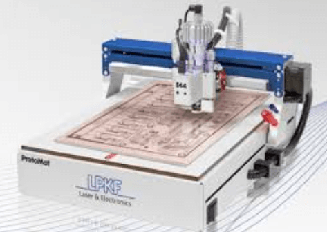
In addition to additive manufacturing, advancements in laser direct imaging (LDI) technology have revolutionized the way PCBs are produced.
LDI uses laser beams to directly transfer the circuit pattern onto the PCB substrate, eliminating the need for photomasks and other intermediate steps. This method significantly improves the precision and resolution of the circuit patterns, allowing for the creation of finer and more intricate designs. Moreover, LDI reduces the turnaround time for PCB production, making it an ideal choice for rapid prototyping applications.
Another critical development in rapid PCB prototyping is the advent of advanced materials, such as flexible and stretchable substrates.
These materials enable the creation of PCBs that can bend, twist, and conform to various shapes, opening up new possibilities for wearable electronics, medical devices, and other applications where traditional rigid PCBs are unsuitable. The use of flexible substrates also enhances the durability and reliability of the PCBs, as they are less prone to damage from mechanical stress and environmental factors.
The integration of advanced design software has also played a pivotal role in the evolution of rapid PCB prototyping.
Modern design tools offer a range of features, including automated routing, real-time simulation, and design rule checking, which streamline the design process and reduce the likelihood of errors. These tools also facilitate collaboration among design teams, enabling them to work together more efficiently and effectively. Additionally, the use of cloud-based platforms allows for seamless sharing and storage of design files, further enhancing the speed and convenience of the prototyping process.
Furthermore, the implementation of machine learning and artificial intelligence (AI) in PCB design and manufacturing has introduced new levels of optimization and automation.
AI algorithms can analyze vast amounts of data to identify patterns and trends, enabling designers to make more informed decisions and optimize their designs for performance, cost, and manufacturability. Machine learning techniques can also be used to predict potential issues and suggest corrective actions, reducing the need for costly and time-consuming iterations.
In conclusion, the advancements in rapid PCB prototyping technologies have significantly transformed the landscape of electronic circuit design and manufacturing. The adoption of additive manufacturing, laser direct imaging, advanced materials, and sophisticated design software has accelerated the development process, improved the precision and quality of PCBs, and expanded the range of possible applications. As these technologies continue to evolve, they will undoubtedly drive further innovation and enable the creation of increasingly complex and high-performance electronic devices.
Benefits Of Rapid PCB Manufacturing For Startups
Rapid PCB manufacturing has emerged as a transformative force in the electronics industry, particularly benefiting startups. This innovative approach to producing printed circuit boards (PCBs) offers numerous advantages that can significantly impact the growth and success of fledgling companies. By understanding these benefits, startups can better position themselves to compete in a fast-paced market.
One of the primary advantages of rapid PCB manufacturing is the accelerated development cycle.
Traditional PCB manufacturing processes can be time-consuming, often taking weeks or even months to complete. In contrast, rapid PCB manufacturing leverages advanced technologies and streamlined processes to produce PCBs in a fraction of the time. This speed is crucial for startups, which often operate under tight deadlines and need to bring their products to market quickly to gain a competitive edge. By reducing the time required for PCB production, startups can iterate on their designs more rapidly, allowing for faster prototyping and testing.
Moreover, rapid PCB manufacturing offers enhanced flexibility, which is particularly beneficial for startups that may need to pivot or make adjustments to their designs.
The ability to quickly produce and test new iterations of a PCB enables startups to respond to market feedback and evolving customer needs more effectively. This adaptability is essential in the early stages of product development, where changes are often necessary to refine and perfect a product. Consequently, startups can avoid costly delays and ensure that their products meet the highest standards of quality and performance.
In addition to speed and flexibility, rapid PCB manufacturing can also lead to cost savings.
Traditional PCB manufacturing often involves high setup costs and large minimum order quantities, which can be prohibitive for startups with limited budgets. Rapid PCB manufacturing, on the other hand, typically allows for smaller production runs and lower setup costs. This affordability enables startups to allocate their resources more efficiently, investing in other critical areas such as marketing, research and development, and talent acquisition. Furthermore, the ability to produce smaller batches reduces the risk of overproduction and excess inventory, which can be a financial burden for startups.
Another significant benefit of rapid PCB manufacturing is the access to advanced technologies and materials.
Startups can leverage cutting-edge manufacturing techniques, such as additive manufacturing and laser direct imaging, to create highly precise and complex PCB designs. These technologies not only improve the overall quality and reliability of the PCBs but also enable startups to explore innovative design possibilities that may not be feasible with traditional manufacturing methods. As a result, startups can differentiate their products in the market and offer unique features that set them apart from competitors.
Additionally, rapid PCB manufacturing often involves close collaboration with experienced manufacturers who can provide valuable insights and guidance throughout the production process.
This partnership can be particularly advantageous for startups that may lack in-house expertise in PCB design and manufacturing. By working with knowledgeable professionals, startups can avoid common pitfalls and ensure that their PCBs are designed and produced to the highest standards. This collaborative approach can also lead to the development of long-term relationships with trusted manufacturing partners, which can be beneficial as the startup grows and scales its operations.
In conclusion, rapid PCB manufacturing offers a multitude of benefits for startups, including accelerated development cycles, enhanced flexibility, cost savings, access to advanced technologies, and valuable industry expertise. By leveraging these advantages, startups can bring their products to market more quickly, respond to customer needs more effectively, and allocate their resources more efficiently. As a result, rapid PCB manufacturing can play a crucial role in the success and growth of startups in the competitive electronics industry.
Cost-Effective Strategies In Rapid PCB Production
In the realm of electronics, the demand for rapid printed circuit board (PCB) manufacturing has surged, driven by the need for swift product development cycles and the constant evolution of technology. As companies strive to bring innovative products to market faster, cost-effective strategies in rapid PCB production have become paramount. These strategies not only ensure timely delivery but also maintain the delicate balance between quality and expenditure.
One of the foremost strategies in achieving cost-effective rapid PCB manufacturing is the adoption of advanced design software.
Modern PCB design tools offer a plethora of features that streamline the design process, reduce errors, and enhance efficiency. By leveraging these tools, designers can simulate and validate their designs before moving to the production phase, thereby minimizing costly revisions and rework. Additionally, these software solutions often include libraries of pre-validated components, which can further expedite the design process and ensure compatibility with manufacturing standards.
Another critical strategy involves the selection of appropriate materials.
The choice of substrate, copper thickness, and solder mask can significantly impact both the cost and performance of the final product. By carefully evaluating the requirements of the application and selecting materials that meet those needs without unnecessary excess, manufacturers can reduce material costs. Moreover, bulk purchasing of commonly used materials can lead to economies of scale, further driving down expenses.
The utilization of automated manufacturing processes is also a key factor in cost-effective rapid PCB production.
Automation not only accelerates production but also enhances precision and consistency, reducing the likelihood of defects. Surface mount technology (SMT) machines, automated optical inspection (AOI) systems, and robotic assembly lines are examples of automation tools that can significantly cut down on labor costs and improve throughput. Furthermore, these technologies enable manufacturers to handle complex designs with high component densities, which are increasingly common in modern electronics.
In addition to automation, the implementation of lean manufacturing principles can lead to substantial cost savings.
Lean manufacturing focuses on eliminating waste, optimizing processes, and improving overall efficiency. By adopting practices such as just-in-time (JIT) inventory management, manufacturers can reduce the costs associated with excess inventory and storage. Continuous improvement initiatives, such as Kaizen, encourage ongoing evaluation and enhancement of production processes, leading to incremental cost reductions over time.
Outsourcing certain aspects of PCB production can also be a viable cost-effective strategy.
Partnering with specialized PCB manufacturers or assembly houses can provide access to advanced technologies and expertise without the need for significant capital investment. These partners often have established relationships with suppliers, enabling them to procure materials at lower costs. Additionally, outsourcing can offer flexibility in scaling production up or down based on demand, thereby avoiding the fixed costs associated with maintaining in-house production capabilities.
Finally, effective communication and collaboration between design and manufacturing teams are essential for cost-effective rapid PCB production.
Early and continuous engagement between these teams can identify potential design-for-manufacturability (DFM) issues, allowing for timely adjustments that prevent costly delays and rework. Utilizing collaborative platforms and tools can facilitate seamless information exchange and ensure that all stakeholders are aligned throughout the production process.
In conclusion, achieving cost-effective rapid PCB manufacturing requires a multifaceted approach that encompasses advanced design tools, strategic material selection, automation, lean manufacturing principles, outsourcing, and effective collaboration. By integrating these strategies, companies can not only accelerate their product development cycles but also maintain a competitive edge in the fast-paced electronics market.
Future Trends In Rapid PCB Manufacturing
The landscape of rapid PCB (Printed Circuit Board) manufacturing is undergoing a significant transformation, driven by technological advancements and evolving market demands. As industries such as consumer electronics, automotive, and telecommunications continue to grow, the need for faster, more efficient PCB production processes becomes increasingly critical. One of the most notable future trends in this domain is the integration of advanced materials and fabrication techniques, which promise to enhance both the performance and reliability of PCBs.
To begin with, the adoption of advanced materials such as flexible substrates and high-frequency laminates is set to revolutionize PCB manufacturing.
Flexible substrates, for instance, allow for the creation of bendable and foldable circuits, which are essential for the development of next-generation wearable devices and flexible displays. High-frequency laminates, on the other hand, are crucial for applications requiring high-speed data transmission, such as 5G networks and advanced radar systems. These materials not only improve the electrical performance of PCBs but also enable the production of more compact and lightweight devices.
In addition to material advancements, the implementation of additive manufacturing techniques, commonly known as 3D printing, is poised to significantly impact the rapid PCB manufacturing industry.
3D printing allows for the layer-by-layer construction of PCBs, which can drastically reduce production times and costs. This technique also offers greater design flexibility, enabling the creation of complex geometries and customized circuit layouts that would be challenging to achieve with traditional subtractive methods. Furthermore, 3D printing can facilitate on-demand manufacturing, reducing the need for large inventories and minimizing waste.
Another emerging trend is the increasing use of automation and artificial intelligence (AI) in PCB manufacturing processes.
Automation technologies, such as robotic assembly and automated optical inspection (AOI), can enhance production efficiency and accuracy by minimizing human error and speeding up repetitive tasks. AI, on the other hand, can be leveraged for predictive maintenance, quality control, and process optimization. By analyzing vast amounts of data from the manufacturing floor, AI algorithms can identify potential issues before they become critical, ensuring higher yields and reducing downtime.
Moreover, the rise of the Internet of Things (IoT) is driving the demand for rapid PCB manufacturing solutions that can support the proliferation of connected devices.
IoT applications often require small, low-power PCBs with integrated sensors and wireless communication capabilities. To meet these requirements, manufacturers are exploring new design methodologies and assembly techniques, such as system-in-package (SiP) and chip-on-board (CoB) technologies. These approaches enable the integration of multiple components into a single, compact module, thereby reducing the overall size and power consumption of IoT devices.
Sustainability is also becoming a key consideration in the future of rapid PCB manufacturing.
As environmental regulations become more stringent and consumer awareness of sustainability issues grows, manufacturers are seeking ways to reduce the environmental impact of their production processes. This includes the development of eco-friendly materials, such as biodegradable substrates and lead-free solder, as well as the implementation of energy-efficient manufacturing practices. Additionally, recycling and reusing PCB materials are gaining traction as viable strategies for minimizing electronic waste.
In conclusion, the future of rapid PCB manufacturing is being shaped by a confluence of technological innovations and market trends. Advanced materials, additive manufacturing, automation, AI, IoT, and sustainability are all playing pivotal roles in driving the evolution of this industry. As these trends continue to develop, they will not only enhance the capabilities and efficiency of PCB production but also open up new possibilities for the design and functionality of electronic devices. Consequently, staying abreast of these advancements will be crucial for manufacturers looking to remain competitive in an increasingly dynamic and demanding market.