Research on CCD signal generator based on CPLD
1 Introduction
CCD (Charge Coupled Devices) is a new type of semiconductor device developed in the early 1970s. At present, CCD is widely used in many fields such as photographic materials, meteorology, aerospace, military, medical treatment and industrial detection as a photoelectric sensor due to its advantages of small size, light weight, low power consumption, low operating voltage and anti-burning, as well as resolution, dynamic range, sensitivity, real-time transmission, self-scanning and other characteristics.
We need to collect and store a large amount of high-speed image data obtained by the CCD camera for subsequent processing and application. Before this series of signal processing, the acquisition of the target signal and the quality of the obtained signal are related to the key to debugging the entire camera system. When debugging the camera system, there are always some imperfect factors in the debugged system, and multiple debugging will also increase the risk cost of the CCD chip.
Especially for the more expensive CCD chip, if it is frequently used during debugging, it will bring the risk of damage. Therefore, the analysis and simulation of the output signal of the CCD chip during the debugging process becomes an extremely important task. This paper designs a programmable broadband and high-precision CCD signal generator based on CPLD. By making full use of the programmability of CPLD, the acquisition signals of CCD in various complex environments are simulated, while meeting the system’s requirements for waveform and timing, and the output signal frequency reaches 11MHz.
2 Analysis of the characteristics of CCD output signals
The output sequence of a CCD signal starts with a reset pulse. When the FET switch is closed, the voltage on the sensor capacitor in Figure 1 is the initial reference voltage value, which is called the reset feedthrough level. After a certain feedthrough delay time, this voltage value decreases and becomes the real reset level. At this time, when the FET switch is turned on, the pixel charge is transferred to this capacitor, which changes the voltage value on the capacitor accordingly. This voltage value is the superposition of the reference level, pixel level and some noise. When the CCD starts to work and read the valid signal, the output signal is reset at the rising edge of each reset signal, that is, a reset interference pulse 1 appears on the output signal, and then returns to the reference level 2, and the pixel signal 3 is obtained by starting to read the integration. The actual pixel width is 3, the sum of the widths of 1, 2, and 3 is a pixel cycle, and the signal amplitude of each pixel is the height difference between 2 and 3. These are important parameters of the CCD output signal. The signal output by the CCD contains a large DC component. The DC bias voltage is indispensable for the normal operation of the CCD. Its value varies from a few volts to more than ten volts, and it consumes only a few milliamperes of current. It can be easily obtained by a voltage regulator through a resistor or potentiometer voltage divider and capacitor filtering when necessary.
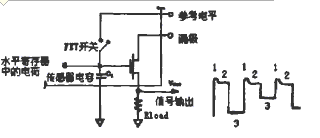
Figure 1 CCD output signal
3 Hardware structure
The entire system consists of three parts: a digital signal generation module, a digital-to-analog conversion module, and an output processing module. CPLD is selected to form the signal generation module, and its programmability is fully utilized to construct the CCD acquisition data in various complex environments. At the same time, a control signal matching the data signal is generated to control the operation of the lower-level digital-to-analog conversion module. The digital-to-analog conversion module receives the data and control signals sent by the upper level, and converts the data into analog signals for output under the control of the control signal. Since the conversion output of this module is current, a conversion module needs to be added to convert the current into the voltage signal required by the system. At the same time, in order to meet the system’s requirements for signal accuracy, active and passive filter circuit modules need to be added. The system block diagram is shown in Figure 2. The crystal oscillator is used as the clock signal (clk) input of the CPLD, and other signals are generated by it.
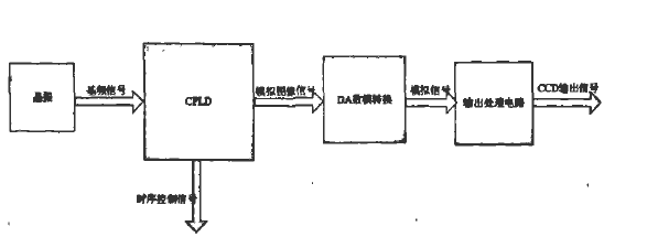
Figure 2 System principle block diagram
The main work is divided into the following aspects:
(1) Signal generation module
Use VHDL language to design CCD output image signal and timing control signal. The output signal includes simulated digital image signal (10-bit parallel output) and timing control signal, mainly including: correlated double sampling signal, timing pulse signal required for A/D sampling, line and field synchronization pulse signal, etc.
(2) Digital-to-analog conversion module
The analog digital signal is converted into an analog signal through a digital-to-analog converter. High-speed digital-to-analog conversion devices generally output current, so the output analog signal needs to be processed later.
(3) Output processing module
The analog signal output by the DAC is converted into a voltage output signal through an op amp, and further processed to obtain a CCD output signal that meets the requirements.
4 Design of the signal generation module CPLD
4.1 Select a CPLD that meets the requirements
This design uses the ispLSI1032e CPLD of LATTICE. The chip has a total of 84 pins, 6000 available gates, 192 logic units, and can be individually configured as input, output, and bidirectional working modes. It has 64 general I/O ports, a transmission delay of 7.5ns, and a maximum operating rate of up to 125MHz, which can meet the requirements of this design. The system requires an output frequency of 11MHz in the form of correlated double sampling CCD signals, and has strict requirements on the timing of the signal. A 66MHz crystal oscillator is selected as the clock input of the CPLD.
4.2 Programming
The output digital signal needs to be provided to the next level sampling system of the image sensor, which meets certain timing requirements and sampling required timing pulse signals. The output signals include analog CCD output signals and correlated double sampling signals, so A/D sampling synchronization pulse signals are required. In the CPLD part of the signal generation module, in addition to generating all digital signals, we also need to prepare the required data and D/A clock timing for the next part of the digital-to-analog conversion module.
In the use of VHDL language to program, simulate and debug in the isp environment, several analog grayscale images and row and field synchronization signals are obtained. The output signals include digital image signals (10-bit parallel output), D/A clock signals (clock1) and write signals (wrt), correlated double sampling signals, row and field synchronization pulse signals, etc. The input clock signal (clk) is 66MHz, and the row synchronization signal row is used to ensure the synchronization of the output pixels.
Its output is used as the clock input of the analog CCD data generation and D/A conversion control module. The square wave signal ccdout[9..0] output by the analog CCD data generation module is converted by DAC to generate the analog output signal of CCD. The D/A conversion control module generates the write signal WR and clock signal CLK of DAC, requiring D/A to sample and convert the high and low levels once in one cycle of data ccdout[9:0]. wrt and clock1 need to sample at the high and low levels of ccdout[9..0] respectively. To ensure the phase relationship between clock1 and wrt signals, the wrt signal is changed on the rising edge of clk, and the clock1 signal is changed on the falling edge of clk, thus generating the data and control signals we need.
4.3 Simulation results
This design realizes the use of VHDL hardware programming language and CPLD to generate the data source signal of the system, including a set of digital signals before the analog signal output by the analog CCD is generated and the control timing required for the next level, ensuring the speed and phase relationship of the system output signal. As shown in the simulation waveform of Figure 3, ccdout[9..0] is the simulated image signal, shp and shd are correlated double sampling signals, and clock1 and wrt are the control signals of the next-level digital-to-analog conversion module D/A. The reference pulse shp and the video pulse shd are sampled once in a pixel interval respectively, and the final output signal is the difference between the reference level and the video level collected. The use of correlated double sampling technology can filter out the reset noise superimposed on the output signal.
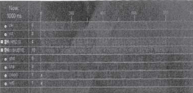
Figure 3 Program simulation results
5 Digital-to-analog conversion and output processing module
DAC2900 is selected as the digital-to-analog converter to convert the simulated grayscale image into an analog signal. DAC2900 is a 10-bit high-speed D/A device produced by TI. DAC2900 uses a single power supply with a power supply range of 3.3-5V. DAC2900 is a current output digital-to-analog converter. It provides differential current output and can support single-ended or differential applications. The matching of the two output currents ensures that the dynamic performance is improved in the differential output structure. The current output can be directly connected to the output resistor to provide two complementary single-ended voltage outputs, or it can be directly input to the transformer.
The analog signal output of DAC2900 can be single-ended output or differential output. The single-ended output connection is relatively simple, but the noise resistance is poor, so the differential output method is adopted to minimize signal noise and electromagnetic interference. In particular, the differential output method can basically cancel out all even harmonics through the positive and negative input signals.
The schematic diagram provided by the DAC2900 chip data is shown in Figure 4, and the reference formula of the configuration scheme is as follows:
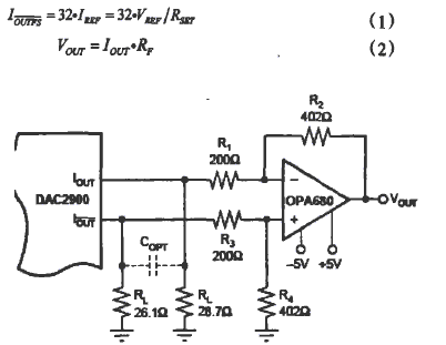
Figure 4 Output processing circuit schematic
Vref is the internal +1.25V reference voltage of DAC2900, and Rset is the configuration resistor value introduced by DAC2900 from the outside. It can be seen from formula (1) that OUTFSI can be adjusted by setting the resistor value, and it can be obtained from formula (2) that the voltage Vout can be controlled. The Rset value of this system is 2K Ω, which can get a full-scale output of 20mA. The system requires a conversion voltage range of 0-500mV, so the output resistance Rf is 25 Ω, which meets the system requirements. CADENCE software is used to implement PCB design, and the schematic diagram is shown in Figure 5:
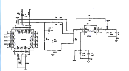
Figure 5 DXP schematic diagram of the digital-to-analog conversion module
6 Improving signal accuracy
After the above-mentioned digital signal generation, digital-to-analog conversion and conversion, the required signal waveform with a frequency of 11 MHz can basically be obtained. A lot of high-frequency noise is superimposed on the signal, which cannot meet the low-noise requirements of the lower-level sampling system. Therefore, it is necessary to improve the signal from multiple angles such as PCB layout, wiring and device configuration to limit the noise to less than 10 mV. The system performance is improved and noise is suppressed mainly from the following three aspects:
(1) Power supply filtering part. Power supply noise is the most harmful. By adding a filter circuit to the power supply part to filter out the power supply noise, and because large bypass capacitors may fail due to resonance, some relatively small bypass capacitor arrays are arranged on the circuit board. Each power supply voltage pin of the CPLD device must be connected to an external 0.1μ capacitor for filtering.
(2) Since the system operates at a higher frequency, the signal integrity problem must be considered, that is, the signal reflection and crosstalk problems between signals must be solved. The series termination method is selected, and the matching resistor is as close to the signal transmitting end as possible. At the same time, the designed PCB diagram is imported into the CADENCE software for simulation to determine the optimal series resistance value. After the actual system is connected in series with the matching resistor, the overshoot and ringing of the signal are effectively eliminated.
(3) Add an analog first-order active filter circuit. Through the oscilloscope, it is found that the generated signal is superimposed with high-frequency noise. In order to filter out the noise, the OPA680 amplifier is selected to form an active low-pass filter circuit. By adjusting the device parameters to change the low-pass frequency range of the filter, the system debugging is greatly facilitated and the high-frequency noise is effectively filtered out. Adding RC low-pass filter circuit to the connector pin has been proven to improve signal quality to a certain extent.
7 Conclusion
After the compilation and simulation are passed, the schematic diagram is used for comprehensive implementation at the top level, and then the chip is burned for experiment, and the design is improved according to the actual operation. For example, according to the delay characteristics of the actual device, appropriate delay units are inserted in certain places in the design to ensure the consistency of each delay. This design completes the CCD output signal simulation and gives the final simulation waveform. We tested the output signal of the designed signal generator under different configuration data. The waveform and signal-to-noise ratio of the signal can fully meet the performance indicators required by the system, which shows that the design scheme is effective.


