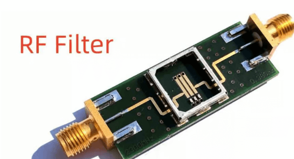
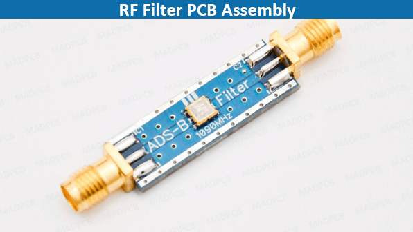
Rf pcb filter
Design Techniques For RF PCB Filters
Designing RF PCB filters is a nuanced process that requires a deep understanding of both theoretical principles and practical considerations. The goal is to create a filter that effectively isolates desired frequencies while attenuating unwanted signals. To achieve this, engineers must employ a variety of design techniques, each tailored to the specific requirements of the application.
One of the first steps in designing an RF PCB filter is selecting the appropriate filter topology.
Common topologies include low-pass, high-pass, band-pass, and band-stop filters. The choice of topology depends on the frequency range that needs to be isolated or attenuated. For instance, a low-pass filter is ideal for applications where high-frequency noise needs to be suppressed, while a band-pass filter is suitable for isolating a specific frequency band.
Once the topology is chosen, the next step involves selecting the right components.
Inductors and capacitors are the building blocks of RF filters, and their values must be carefully calculated to achieve the desired frequency response. The quality of these components is crucial; high-Q inductors and capacitors with low equivalent series resistance (ESR) are preferred to minimize losses and ensure efficient signal transmission.
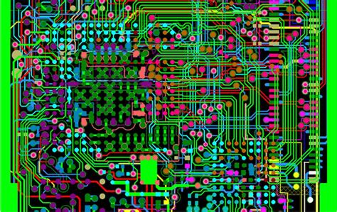
In addition to component selection, the layout of the PCB plays a critical role in the performance of the RF filter.
Parasitic elements such as stray capacitance and inductance can significantly affect the filter’s behavior. To mitigate these effects, designers must pay close attention to the placement of components and the routing of traces. For example, keeping signal paths as short as possible and using ground planes can help reduce parasitic inductance and capacitance.
Moreover, the choice of substrate material can also impact the filter’s performance.
Materials with low dielectric loss and stable dielectric constants are preferred for high-frequency applications. Rogers and Teflon-based substrates are commonly used in RF PCB designs due to their excellent electrical properties. However, these materials can be more expensive than standard FR4, so cost considerations must also be taken into account.
Thermal management is another important aspect of RF PCB filter design.
High-frequency signals can generate significant heat, which can affect the performance and reliability of the filter. To address this, designers can use thermal vias and heat sinks to dissipate heat effectively. Additionally, ensuring adequate spacing between components can help prevent thermal coupling and reduce the risk of overheating.
Simulation tools are invaluable in the design process, allowing engineers to model the filter’s behavior before committing to a physical prototype.
Software such as SPICE and electromagnetic simulation tools can provide insights into the filter’s frequency response, insertion loss, and return loss. By iterating on the design in the simulation phase, engineers can optimize the filter’s performance and identify potential issues early on.
Finally, once the design is finalized, thorough testing is essential to validate the filter’s performance.
Network analyzers can be used to measure key parameters such as insertion loss, return loss, and bandwidth. Any discrepancies between the simulated and measured results can be addressed through fine-tuning the design or adjusting component values.
In conclusion, designing RF PCB filters is a complex but rewarding endeavor that requires careful consideration of various factors. By selecting the appropriate topology, choosing high-quality components, optimizing the PCB layout, and leveraging simulation tools, engineers can create filters that meet the stringent demands of modern RF applications. Through meticulous design and testing, it is possible to achieve high-performance RF filters that enhance the overall functionality and reliability of electronic systems.
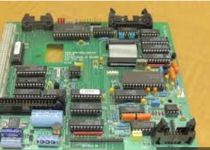
Common Challenges In RF PCB Filter Implementation
Implementing RF PCB filters presents a myriad of challenges that can significantly impact the performance and reliability of the final product.
One of the primary difficulties lies in the precise design and layout of the filter.
RF signals are highly sensitive to even the smallest variations in component placement and trace routing. Consequently, achieving the desired filter characteristics requires meticulous attention to detail during the design phase. Any deviation from the intended layout can result in unwanted signal attenuation or interference, thereby compromising the filter’s effectiveness.
Another common challenge is the selection of appropriate materials.
The dielectric properties of the PCB substrate play a crucial role in determining the filter’s performance. Materials with high dielectric constants can lead to increased signal loss and reduced filter efficiency. Therefore, choosing the right substrate material is essential to ensure optimal performance. Additionally, the thermal properties of the materials must be considered, as RF circuits often generate significant heat. Inadequate thermal management can lead to component failure and reduced filter lifespan.
Moreover, the integration of RF PCB filters into larger systems introduces additional complexities.
Ensuring compatibility with other components and maintaining signal integrity across the entire system can be daunting. The presence of other high-frequency signals can cause crosstalk and electromagnetic interference (EMI), which can degrade the filter’s performance. To mitigate these issues, designers must employ effective shielding and grounding techniques. Proper isolation of the RF filter from other circuit elements is crucial to prevent unwanted interactions and maintain signal purity.
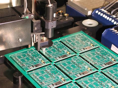
Furthermore, the manufacturing process itself poses significant challenges.
The precision required in fabricating RF PCB filters demands advanced manufacturing techniques and equipment. Variations in the etching process, for instance, can lead to discrepancies in trace widths and spacing, affecting the filter’s performance. Ensuring consistent quality across multiple production runs is essential to maintain reliability. This necessitates stringent quality control measures and thorough testing to identify and rectify any deviations from the desired specifications.
In addition to these technical challenges, cost considerations also play a pivotal role.
High-performance RF PCB filters often require specialized materials and manufacturing processes, which can drive up production costs. Balancing performance requirements with budget constraints is a delicate task. Designers must carefully evaluate the trade-offs between cost and performance to achieve an optimal solution. This often involves iterative design and testing cycles to fine-tune the filter characteristics while keeping costs in check.
Moreover, the rapid pace of technological advancements adds another layer of complexity.
As new communication standards and frequency bands emerge, RF PCB filter designs must evolve to meet these changing requirements. Staying abreast of the latest developments and incorporating them into the design process is essential to ensure future-proof solutions. This necessitates continuous learning and adaptation, as well as close collaboration with component manufacturers and industry experts.
In conclusion, implementing RF PCB filters is fraught with challenges that span design, material selection, system integration, manufacturing, cost management, and technological evolution. Overcoming these hurdles requires a comprehensive understanding of RF principles, meticulous attention to detail, and a proactive approach to problem-solving. By addressing these challenges head-on, designers can develop robust and reliable RF PCB filters that meet the stringent demands of modern communication systems.
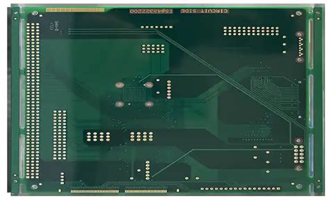
Materials And Components For High-Performance RF PCB Filters
When designing high-performance RF PCB filters, the choice of materials and components is paramount to achieving optimal performance. The intricate nature of RF signals, which operate at high frequencies, necessitates the use of specialized materials that can handle the demands of such applications.
One of the primary considerations is the substrate material, which forms the foundation of the PCB.
High-frequency laminates, such as Rogers RO4000 series or Taconic RF-35, are often preferred due to their low dielectric constant and minimal loss tangent. These properties ensure minimal signal loss and maintain signal integrity, which is crucial for RF applications.
In addition to the substrate, the selection of conductive materials plays a significant role.
Copper is the most commonly used conductor due to its excellent electrical conductivity and relatively low cost. However, for high-performance RF PCB filters, the quality of the copper foil is critical. Electrodeposited copper, with its smooth surface finish, is often chosen over rolled copper to reduce signal attenuation and improve overall performance. Furthermore, the thickness of the copper layer must be carefully considered, as it impacts the impedance and current-carrying capacity of the traces.
Transitioning to the components, the choice of capacitors and inductors is equally important.
Surface-mount technology (SMT) components are typically used in RF PCB filters due to their compact size and ease of assembly. High-Q capacitors, such as those made from ceramic materials, are favored for their low equivalent series resistance (ESR) and high self-resonant frequency (SRF). These characteristics are essential for maintaining signal purity and minimizing losses. Similarly, inductors with high Q-factors and low parasitic capacitance are selected to ensure efficient energy storage and transfer.
Moreover, the layout and design of the PCB itself are critical to the performance of RF filters.
Proper grounding and shielding techniques must be employed to prevent electromagnetic interference (EMI) and crosstalk between adjacent traces. Utilizing ground planes and via stitching can significantly enhance the isolation and reduce unwanted noise. Additionally, the trace width and spacing must be meticulously calculated to match the desired impedance and minimize signal reflections.
Another vital aspect to consider is the thermal management of the RF PCB filter.
High-frequency signals can generate significant heat, which, if not properly managed, can degrade the performance and reliability of the filter. Using materials with good thermal conductivity, such as metal-backed substrates or incorporating thermal vias, can help dissipate heat effectively. Furthermore, careful placement of heat-generating components and the use of thermal relief pads can prevent hotspots and ensure uniform temperature distribution.
In conclusion, the materials and components used in high-performance RF PCB filters are crucial to their success. From the choice of substrate and conductive materials to the selection of capacitors and inductors, each element must be carefully considered to achieve optimal performance. Additionally, the layout, design, and thermal management of the PCB play significant roles in ensuring the filter’s efficiency and reliability. By paying close attention to these factors, designers can create RF PCB filters that meet the stringent demands of high-frequency applications, ensuring signal integrity and minimizing losses.

Testing And Tuning Methods For RF PCB Filters
Testing and tuning methods for RF PCB filters are crucial steps in ensuring optimal performance and reliability in various applications. These filters, which are integral components in wireless communication systems, must be meticulously evaluated and adjusted to meet stringent specifications. The process begins with a thorough understanding of the filter’s design parameters and intended operational environment. This foundational knowledge guides the selection of appropriate testing equipment and methodologies.
Initially, the RF PCB filter undergoes a series of preliminary tests to verify its basic functionality.
These tests typically include measuring the insertion loss, return loss, and bandwidth. Insertion loss, which quantifies the signal attenuation as it passes through the filter, is a critical parameter. A network analyzer is commonly used to measure this loss, providing a clear indication of the filter’s efficiency. Similarly, return loss, which measures the amount of signal reflected back towards the source, is assessed to ensure minimal signal degradation. A high return loss value indicates good impedance matching, which is essential for maintaining signal integrity.
Once the preliminary tests confirm the filter’s basic performance, more detailed evaluations are conducted.
These include examining the filter’s frequency response, which is crucial for determining its ability to pass desired frequencies while attenuating unwanted ones. A spectrum analyzer is often employed for this purpose, allowing for precise visualization of the filter’s behavior across a range of frequencies. Additionally, the filter’s phase response is analyzed to ensure that it does not introduce unwanted phase shifts, which could distort the signal.
After the initial testing phase, the tuning process begins.
Tuning an RF PCB filter involves making fine adjustments to its components to achieve the desired performance characteristics. This process is iterative and requires a deep understanding of the filter’s design and the interplay between its various elements. For instance, adjusting the values of capacitors and inductors can significantly impact the filter’s frequency response and impedance matching. Therefore, careful consideration is given to each adjustment, with continuous monitoring of the filter’s performance using the aforementioned testing equipment.
Throughout the tuning process, it is essential to maintain a controlled environment to ensure consistent and accurate results.
Factors such as temperature, humidity, and electromagnetic interference can affect the filter’s performance, leading to erroneous conclusions. Therefore, testing and tuning are typically conducted in specialized laboratories equipped with environmental controls and shielding to mitigate these influences.
Moreover, advanced simulation tools play a pivotal role in the testing and tuning of RF PCB filters.
These tools allow engineers to model the filter’s behavior under various conditions, providing valuable insights that guide the tuning process. By comparing the simulated results with actual measurements, engineers can identify discrepancies and make informed adjustments to the filter’s design.
In conclusion, the testing and tuning of RF PCB filters are intricate processes that demand a combination of precise measurements, iterative adjustments, and environmental controls. By employing a systematic approach and leveraging advanced tools, engineers can ensure that these filters meet the required performance standards, thereby enhancing the reliability and efficiency of wireless communication systems. The meticulous nature of these processes underscores the importance of expertise and attention to detail in the field of RF engineering.