Rf pcb routing
Best Practices For RF PCB Routing
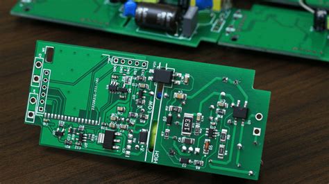
Routing printed circuit boards (PCBs) for radio frequency (RF) applications presents unique challenges that require careful consideration and meticulous planning. The performance of RF circuits is highly sensitive to layout, and even minor deviations can lead to significant issues such as signal loss, interference, and impedance mismatches. Therefore, adhering to best practices in RF PCB routing is crucial to ensure optimal functionality and reliability.
To begin with, understanding the importance of impedance control is fundamental.
RF signals are particularly susceptible to impedance mismatches, which can cause reflections and degrade signal integrity. To mitigate this, it is essential to maintain consistent trace widths and spacing, as well as to use appropriate dielectric materials. Calculating the characteristic impedance of transmission lines and ensuring it matches the source and load impedance is a critical step in the design process. Utilizing tools such as impedance calculators and simulation software can aid in achieving the desired impedance levels.
Moreover, minimizing signal path lengths is another key consideration.
Shorter signal paths reduce the potential for signal degradation and minimize the effects of parasitic inductance and capacitance. This can be achieved by placing components as close together as possible and by using direct routing paths. Additionally, avoiding unnecessary vias is advisable, as they can introduce unwanted inductance and disrupt the signal flow. When vias are unavoidable, using blind or buried vias can help minimize their impact.
Transitioning to the topic of grounding, a solid grounding strategy is indispensable for RF PCB routing.
A continuous ground plane is recommended to provide a low-inductance return path for RF signals, which helps in reducing electromagnetic interference (EMI) and maintaining signal integrity. It is also beneficial to use multiple ground vias to connect the ground plane to the top and bottom layers of the PCB, thereby ensuring a robust ground connection. Furthermore, separating analog and digital grounds can prevent noise coupling between different circuit sections.
In addition to grounding, shielding is another effective technique to enhance RF performance.
Shielding can be implemented through the use of ground traces or guard traces around sensitive signal lines. These traces act as barriers, preventing external noise from coupling into the RF signals. Moreover, placing critical RF components within shielded enclosures can further protect them from external interference.
Another aspect to consider is the use of differential signaling for RF signals, which can offer significant advantages in terms of noise immunity and signal integrity.
Differential pairs should be routed symmetrically and with equal lengths to maintain signal balance. This approach helps in canceling out common-mode noise and improving overall performance.
Finally, thermal management should not be overlooked in RF PCB routing.
High-frequency components can generate significant heat, which can affect performance and reliability. Implementing thermal vias, heat sinks, and adequate copper pours can help dissipate heat effectively. Additionally, ensuring that components are not placed too closely together can prevent thermal coupling and overheating.
In conclusion, RF PCB routing demands a comprehensive understanding of various factors that influence signal integrity and performance.
By adhering to best practices such as impedance control, minimizing signal path lengths, implementing effective grounding and shielding strategies, utilizing differential signaling, and managing thermal issues, designers can create RF PCBs that meet the stringent requirements of modern RF applications. These practices not only enhance the performance of RF circuits but also contribute to the overall reliability and longevity of the electronic systems in which they are employed.
Common Mistakes In RF PCB Design
In the realm of RF PCB design, precision and attention to detail are paramount. However, even seasoned engineers can fall prey to common mistakes that can compromise the performance and reliability of the final product. Understanding these pitfalls is crucial for anyone involved in the design and development of RF PCBs.
One of the most frequent errors is the improper management of impedance.
RF signals are highly sensitive to impedance mismatches, which can lead to signal reflections and loss. To mitigate this, designers must ensure that transmission lines are carefully matched to the characteristic impedance of the system. This involves meticulous calculations and the use of appropriate materials and geometries to maintain consistent impedance throughout the circuit.
Another prevalent mistake is inadequate grounding.
A robust grounding strategy is essential for minimizing electromagnetic interference (EMI) and ensuring signal integrity. Designers often overlook the importance of a solid ground plane, which can result in increased noise and crosstalk. To avoid this, it is advisable to use a continuous ground plane and to minimize the number of vias that can disrupt the ground path. Additionally, ensuring that all components have a low-impedance connection to the ground plane can significantly enhance the performance of the RF PCB.
Furthermore, the placement of components is a critical aspect that can greatly influence the functionality of an RF PCB.
Poor component placement can lead to unwanted coupling and interference between different parts of the circuit. It is essential to place sensitive components, such as oscillators and amplifiers, away from noisy digital circuits. Moreover, maintaining adequate spacing between components can help reduce parasitic capacitance and inductance, which are detrimental to high-frequency performance.
Transitioning to another common oversight, the routing of traces is often mishandled. RF signals require careful routing to prevent signal degradation.
Sharp bends and long trace lengths can introduce inductance and capacitance, which can distort the signal. To address this, designers should aim for smooth, gradual curves and keep trace lengths as short as possible. Additionally, using microstrip or stripline configurations can help maintain signal integrity by providing controlled impedance paths.
In addition to these technical considerations, thermal management is another area where mistakes frequently occur.
RF components can generate significant heat, which, if not properly managed, can lead to performance issues or even component failure. Designers should incorporate adequate thermal vias and heat sinks to dissipate heat effectively. Moreover, selecting materials with good thermal conductivity can aid in maintaining optimal operating temperatures.
Lastly, neglecting to perform thorough testing and validation is a mistake that can have serious repercussions.
Even the most meticulously designed RF PCB can harbor unforeseen issues that only become apparent during testing. Comprehensive testing, including signal integrity analysis and EMI testing, is essential to identify and rectify potential problems before mass production.
In conclusion, while RF PCB design presents numerous challenges, being aware of and addressing these common mistakes can significantly enhance the performance and reliability of the final product. By focusing on impedance matching, grounding, component placement, trace routing, thermal management, and thorough testing, designers can avoid the pitfalls that often plague RF PCB projects. Through careful planning and execution, it is possible to achieve a design that meets the stringent demands of modern RF applications.

Advanced Techniques For RF Signal Integrity
In the realm of radio frequency (RF) design, maintaining signal integrity is paramount, particularly when dealing with printed circuit boards (PCBs). As RF technology continues to evolve, the complexity of PCB routing has increased, necessitating advanced techniques to ensure optimal performance. One of the primary challenges in RF PCB routing is minimizing signal loss and interference, which can significantly degrade the performance of RF circuits. To address these challenges, engineers employ a variety of sophisticated strategies that enhance signal integrity.
Firstly, understanding the importance of impedance matching is crucial.
Impedance mismatches can lead to signal reflections, which in turn cause loss and distortion. To mitigate this, designers must carefully calculate and maintain consistent impedance throughout the RF path. This involves selecting appropriate trace widths and dielectric materials, as well as considering the effects of vias and connectors. By ensuring that the impedance is matched across all components, signal reflections can be minimized, thereby preserving signal integrity.
Moreover, the layout of the PCB plays a critical role in maintaining RF signal integrity.
The placement of components should be strategically planned to minimize the length of RF traces, as longer traces can act as antennas, picking up unwanted noise and interference. Additionally, the use of ground planes is essential in RF PCB design. Ground planes provide a return path for RF signals and help to shield sensitive components from electromagnetic interference (EMI). By carefully designing the ground plane layout, engineers can reduce the potential for crosstalk and other forms of interference.
Transitioning to the topic of trace routing, it is important to consider the use of microstrip and stripline configurations.
Microstrip lines, which are traces on the outer layer of the PCB, are often used for their simplicity and ease of access. However, they are more susceptible to external interference. In contrast, stripline configurations, which are sandwiched between two ground planes, offer better isolation and are preferred for high-frequency applications. The choice between these configurations depends on the specific requirements of the RF design, including frequency range and environmental conditions.
Another advanced technique involves the use of via stitching.
Vias are used to connect different layers of a PCB, but they can introduce inductance and capacitance, affecting signal integrity. Via stitching involves placing multiple vias around RF traces to create a more uniform ground return path. This technique helps to reduce the inductive effects of individual vias and improves the overall performance of the RF circuit.
Furthermore, the selection of materials is a critical consideration in RF PCB routing.
The dielectric constant and loss tangent of the substrate material can significantly impact signal propagation. Low-loss materials are preferred for high-frequency applications to minimize signal attenuation. Additionally, the thermal properties of the material should be considered, as RF circuits can generate significant heat, which may affect performance and reliability.
In conclusion, maintaining RF signal integrity in PCB routing requires a comprehensive understanding of various advanced techniques. From impedance matching and strategic component placement to the careful selection of materials and routing configurations, each aspect plays a vital role in ensuring optimal performance. As RF technology continues to advance, the demand for innovative solutions in PCB design will only grow, making it essential for engineers to stay abreast of the latest developments in this dynamic field.

Material Selection For RF PCB Applications
In the realm of RF PCB routing, the selection of materials plays a pivotal role in determining the performance and reliability of the final product. As RF applications continue to evolve, demanding higher frequencies and more complex functionalities, the importance of choosing the right materials cannot be overstated. The intricate nature of RF signals, which are highly sensitive to interference and loss, necessitates a careful consideration of the substrate materials used in PCB fabrication.
To begin with, one of the primary considerations in material selection for RF PCBs is the dielectric constant (Dk).
The dielectric constant affects the speed at which signals propagate through the material, and thus, it is crucial to select a material with a stable Dk over the desired frequency range. Materials with a low and stable dielectric constant are often preferred as they minimize signal delay and dispersion, ensuring signal integrity. Furthermore, the loss tangent, or dissipation factor, is another critical parameter. A low loss tangent is desirable as it indicates that the material will have minimal dielectric losses, which is essential for maintaining signal strength and reducing power consumption in RF applications.
In addition to electrical properties, thermal management is a significant factor in material selection.
RF circuits often generate substantial heat, and the ability of a material to dissipate this heat can impact the performance and longevity of the PCB. Therefore, materials with high thermal conductivity are advantageous as they facilitate efficient heat dissipation, preventing overheating and potential damage to the components. Moreover, the coefficient of thermal expansion (CTE) should be compatible with other materials used in the PCB to avoid mechanical stress and potential failure during thermal cycling.
Another aspect to consider is the mechanical properties of the substrate material.
RF PCBs are often subjected to various environmental conditions, including vibration and mechanical stress. Therefore, materials with robust mechanical properties are essential to ensure the structural integrity and durability of the PCB. Additionally, the material should be easy to process and compatible with standard PCB manufacturing techniques to ensure cost-effectiveness and scalability.
Furthermore, the choice of material can also be influenced by regulatory and environmental considerations.
With increasing emphasis on sustainability and environmental responsibility, selecting materials that comply with environmental regulations, such as RoHS (Restriction of Hazardous Substances), is becoming increasingly important. This not only ensures compliance with legal requirements but also aligns with the growing demand for environmentally friendly products.
In conclusion, the selection of materials for RF PCB applications is a multifaceted decision that requires a careful balance of electrical, thermal, mechanical, and environmental considerations. As RF technologies continue to advance, the demand for materials that can meet the stringent requirements of high-frequency applications will only increase. By understanding the critical parameters and trade-offs involved in material selection, designers can make informed decisions that enhance the performance, reliability, and sustainability of RF PCBs. Ultimately, the right material choice is instrumental in achieving the desired performance outcomes and ensuring the success of RF applications in an increasingly complex and demanding technological landscape.


