Rf pcb test probe
Understanding The Basics Of RF PCB Test Probes
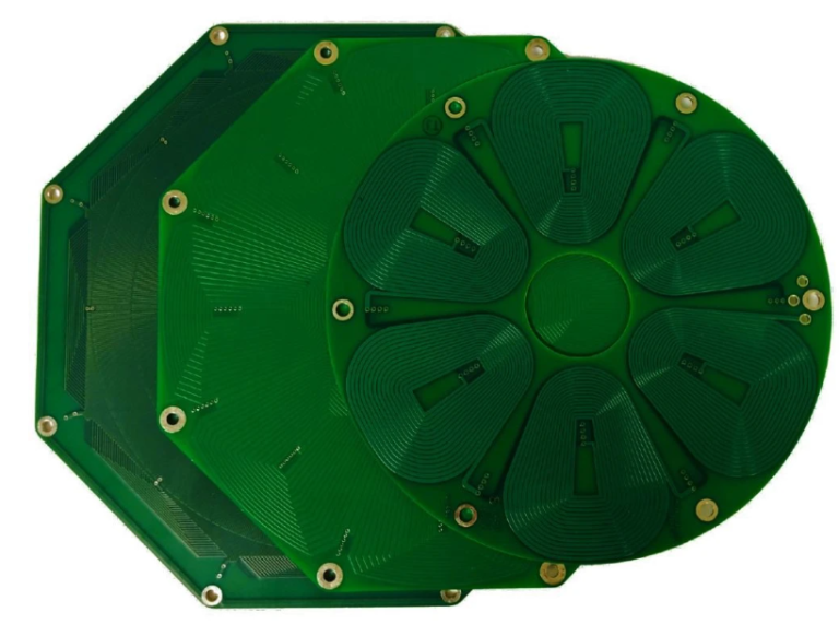
RF PCB test probes are essential tools in the realm of electronics, particularly in the testing and validation of radio frequency (RF) printed circuit boards (PCBs). These probes are designed to facilitate the accurate measurement and analysis of high-frequency signals, ensuring that the PCBs function correctly within their intended applications. Understanding the basics of RF PCB test probes involves delving into their design, functionality, and the critical role they play in the electronics industry.
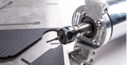
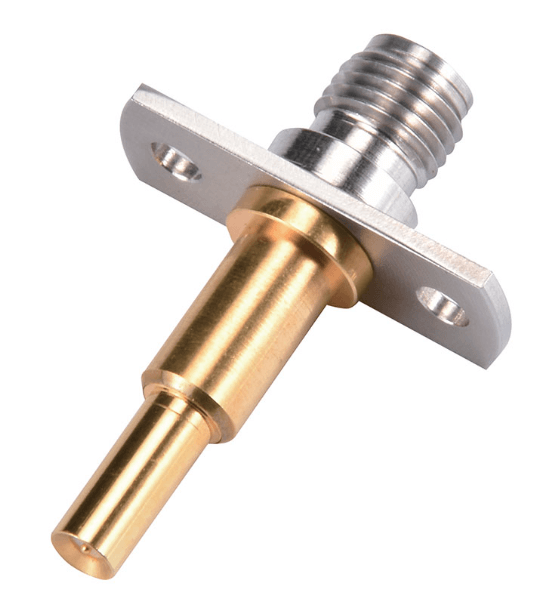
To begin with, RF PCB test probes are specialized devices that connect test equipment to the PCB under examination.
They are engineered to handle the unique challenges posed by high-frequency signals, which can range from a few megahertz (MHz) to several gigahertz (GHz). The design of these probes is crucial, as it must minimize signal loss and interference, which can otherwise lead to inaccurate measurements. Typically, RF PCB test probes feature a coaxial structure, which helps maintain signal integrity by providing a consistent impedance path from the probe tip to the test equipment.
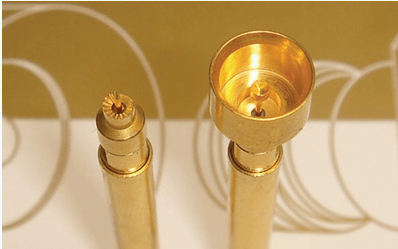
Moreover, the materials used in the construction of RF PCB test probes are selected for their ability to handle high frequencies.
Conductive materials such as gold or beryllium copper are often used for the probe tips, as they offer excellent electrical conductivity and durability. The body of the probe is usually made from materials with low dielectric constants, such as PTFE (polytetrafluoroethylene), to reduce signal attenuation and ensure reliable performance.
In addition to their construction, the functionality of RF PCB test probes is another critical aspect to consider.
These probes are designed to make contact with specific test points on the PCB, allowing engineers to measure parameters such as signal amplitude, phase, and frequency response. The precision of these measurements is paramount, as even minor deviations can significantly impact the performance of RF circuits. Therefore, RF PCB test probes must provide a stable and repeatable connection to the test points, minimizing any potential sources of error.
Furthermore, the role of RF PCB test probes extends beyond mere measurement.
They are also instrumental in the debugging and troubleshooting of RF circuits. When a PCB fails to meet its performance specifications, engineers can use RF PCB test probes to identify and isolate the source of the problem. By systematically probing different points on the PCB, they can pinpoint issues such as signal reflections, impedance mismatches, or component failures. This diagnostic capability is invaluable in the development and refinement of RF circuits, ensuring that they meet the stringent requirements of modern electronic systems.
Transitioning to the practical applications of RF PCB test probes, it is evident that they are indispensable in various industries.
In telecommunications, for instance, these probes are used to test the performance of RF components in mobile phones, base stations, and satellite communication systems. Similarly, in the aerospace and defense sectors, RF PCB test probes play a crucial role in the development and maintenance of radar systems, communication equipment, and electronic warfare devices. The automotive industry also relies on these probes to ensure the reliability of RF systems used in vehicle-to-vehicle communication and advanced driver-assistance systems (ADAS).
In conclusion, RF PCB test probes are vital tools that enable the accurate testing and validation of high-frequency PCBs. Their specialized design and functionality ensure that engineers can obtain precise measurements and diagnose issues effectively. As technology continues to advance, the importance of RF PCB test probes in ensuring the performance and reliability of electronic systems cannot be overstated.
Top Techniques For Effective RF PCB Test Probe Usage
Effective usage of RF PCB test probes is crucial for ensuring the reliability and performance of radio frequency printed circuit boards. These probes are essential tools for engineers and technicians, enabling them to measure and analyze the electrical characteristics of RF circuits with precision. To achieve optimal results, it is important to employ top techniques that enhance the accuracy and efficiency of RF PCB test probe usage.
One of the primary techniques involves selecting the appropriate test probe for the specific application.
RF PCB test probes come in various types, each designed for different frequency ranges and signal characteristics. For instance, high-frequency probes are necessary for applications involving gigahertz signals, while lower-frequency probes may suffice for megahertz ranges. By carefully matching the probe to the frequency requirements of the circuit, users can minimize signal distortion and ensure accurate measurements.
Another critical technique is proper probe placement.
The position of the test probe on the PCB can significantly impact the measurement results.
Ideally, the probe should be placed as close as possible to the point of interest to reduce the effects of parasitic inductance and capacitance. Additionally, maintaining a consistent and stable contact with the test point is essential to avoid intermittent connections that could lead to erroneous readings. Using probe holders or fixtures can help achieve this stability, ensuring reliable and repeatable measurements.
Furthermore, minimizing signal interference is a key consideration when using RF PCB test probes.
Electromagnetic interference (EMI) and crosstalk from adjacent circuits can introduce noise and distort the measured signals. To mitigate these effects, it is advisable to use shielded probes and cables, which can effectively block external noise sources. Additionally, keeping the test setup as compact as possible and avoiding long cable runs can further reduce the potential for interference.
Calibration is another vital aspect of effective RF PCB test probe usage.
Regular calibration of the test probes and associated measurement equipment ensures that the readings remain accurate over time. Calibration involves comparing the probe’s measurements against known standards and making necessary adjustments to account for any deviations. By adhering to a strict calibration schedule, users can maintain the integrity of their measurements and avoid potential discrepancies.
Moreover, understanding the limitations of the test probes is essential for accurate data interpretation.
Each probe has a specified bandwidth, input impedance, and voltage rating, which define its operational boundaries. Exceeding these limits can result in measurement errors or even damage to the probe and the circuit under test. Therefore, it is crucial to consult the manufacturer’s specifications and ensure that the probe is used within its designated parameters.
In addition to these techniques, proper handling and maintenance of RF PCB test probes are fundamental to their longevity and performance. Probes should be stored in protective cases when not in use to prevent physical damage and contamination. Regular inspection for wear and tear, such as bent or broken tips, is also necessary to ensure reliable contact with the test points. Cleaning the probe tips with appropriate solvents can remove any accumulated debris, further enhancing measurement accuracy.
In conclusion, effective RF PCB test probe usage requires a combination of careful probe selection, precise placement, interference minimization, regular calibration, and proper handling. By adhering to these top techniques, engineers and technicians can achieve accurate and reliable measurements, ultimately ensuring the optimal performance of RF circuits.
Common Challenges In RF PCB Test Probing And How To Overcome Them
Testing radio frequency (RF) printed circuit boards (PCBs) presents a unique set of challenges that can significantly impact the accuracy and reliability of the results.
One of the primary difficulties encountered in RF PCB test probing is maintaining signal integrity.
RF signals are highly susceptible to interference and loss, which can be exacerbated by improper probing techniques. To mitigate this issue, it is essential to use high-quality RF test probes specifically designed to handle high-frequency signals. These probes should have minimal insertion loss and return loss to ensure that the signal remains as true to its original form as possible.
Another common challenge is the physical accessibility of the test points on the PCB.
RF circuits often require compact and intricate layouts to function effectively, which can make it difficult to place test probes without disturbing the surrounding components. To address this, engineers can employ specialized test fixtures that provide stable and repeatable connections to the test points. These fixtures can be custom-designed to fit the specific layout of the PCB, ensuring that the probes make consistent contact with the test points without causing any mechanical stress or damage to the board.
Thermal management is also a critical concern in RF PCB test probing.
High-frequency signals can generate significant amounts of heat, which can affect the performance of both the PCB and the test equipment. To overcome this, it is important to implement effective cooling solutions, such as heat sinks or active cooling systems, to dissipate the heat generated during testing. Additionally, using probes with low thermal mass can help minimize the impact of temperature fluctuations on the test results.
The accuracy of the test measurements can be further compromised by the presence of parasitic elements, such as stray capacitance and inductance, which can introduce errors into the readings.
To reduce the influence of these parasitic elements, it is crucial to use probes with a high degree of electrical isolation and shielding. This helps to minimize the coupling of unwanted signals and ensures that the measurements reflect the true performance of the RF circuit.
Calibration is another vital aspect of RF PCB test probing that cannot be overlooked.
Accurate calibration of the test equipment and probes is essential to obtain reliable and repeatable results. This involves using precision calibration standards and following a rigorous calibration procedure to account for any variations in the test setup. Regular calibration checks should be performed to ensure that the equipment remains within the specified tolerances and continues to provide accurate measurements.
Finally, the complexity of modern RF circuits often necessitates the use of advanced test methodologies,
such as vector network analysis (VNA) and time-domain reflectometry (TDR), to fully characterize the performance of the PCB. These techniques require specialized equipment and expertise to interpret the results correctly. Investing in training and staying up-to-date with the latest advancements in RF testing technology can help engineers effectively address the challenges associated with RF PCB test probing.
In conclusion, overcoming the common challenges in RF PCB test probing requires a combination of high-quality test probes, effective thermal management, careful consideration of parasitic elements, rigorous calibration procedures, and advanced test methodologies. By addressing these factors, engineers can ensure that their RF PCB testing yields accurate and reliable results, ultimately leading to better-performing RF circuits and systems.
Innovations In RF PCB Test Probe Technology
The field of radio frequency (RF) technology has seen significant advancements over the past few decades, and one of the critical components in this domain is the RF printed circuit board (PCB) test probe. These test probes are essential for ensuring the functionality and reliability of RF circuits, which are integral to a wide range of applications, from telecommunications to aerospace. Innovations in RF PCB test probe technology have been pivotal in enhancing the accuracy, efficiency, and overall performance of RF testing processes.
One of the most notable advancements in RF PCB test probe technology is the development of high-frequency probes capable of operating at gigahertz frequencies.
Traditional test probes often struggled with signal integrity issues at higher frequencies, leading to inaccurate measurements and potential design flaws. However, modern RF PCB test probes are designed with advanced materials and precision engineering to minimize signal loss and reflection, thereby providing more reliable data. This improvement is particularly crucial for applications such as 5G communications and satellite systems, where even minor discrepancies can have significant consequences.
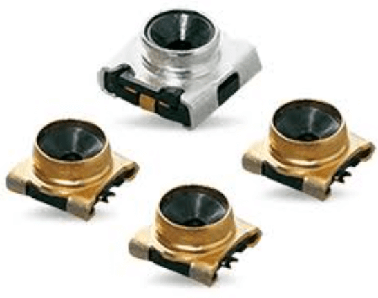
In addition to frequency capabilities, the miniaturization of RF PCB test probes has been a significant innovation.
As electronic devices become increasingly compact, the need for smaller and more precise test probes has grown. Engineers have responded by developing probes with finer tips and more robust construction, allowing for accurate testing of densely packed PCBs without damaging the delicate components. This miniaturization has been facilitated by advancements in microfabrication techniques and materials science, enabling the production of probes that can access even the most confined spaces on a PCB.
Another critical area of innovation is the integration of automated testing systems with RF PCB test probes.
Automation has revolutionized many aspects of electronics manufacturing, and RF testing is no exception. Automated test systems equipped with advanced RF probes can perform complex testing sequences with minimal human intervention, significantly reducing the time and cost associated with manual testing. These systems can also provide more consistent and repeatable results, enhancing the overall reliability of the testing process. The integration of machine learning algorithms further augments these systems, enabling them to adapt to new testing scenarios and optimize their performance over time.
Moreover, the development of multi-functional RF PCB test probes has expanded the capabilities of testing equipment.
These probes can perform multiple types of measurements simultaneously, such as impedance, capacitance, and signal integrity, providing a comprehensive assessment of the PCB’s performance. This multi-functionality not only streamlines the testing process but also reduces the need for multiple probes and testing setups, thereby saving space and resources in the testing environment.
The use of advanced simulation and modeling tools has also played a crucial role in the innovation of RF PCB test probes.
Engineers can now design and test probe prototypes in virtual environments before physical production, allowing for rapid iteration and optimization. This approach reduces development time and costs while ensuring that the final product meets the stringent requirements of modern RF applications.
In conclusion, the innovations in RF PCB test probe technology have significantly enhanced the capabilities and efficiency of RF testing processes. High-frequency operation, miniaturization, automation, multi-functionality, and advanced simulation tools are among the key advancements that have driven this progress. As RF technology continues to evolve, the ongoing development of sophisticated test probes will remain essential to ensuring the reliability and performance of RF circuits across various industries.