Routing strategy in PCB Layout
Layout is one of the most basic working skills of PCB design engineers. The quality of routing will directly affect the performance of the entire system. Most high-speed design theories must eventually be implemented and verified through Layout. It can be seen that routing is crucial in high-speed PCB design. The following will analyze the rationality of some situations that may be encountered in actual routing, and give some relatively optimized routing strategies. It is mainly explained from three aspects: right-angle routing, differential routing, and serpentine routing.
1.Right-angle routing
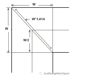
Right-angle routing is generally a situation that is required to be avoided as much as possible in PCB routing, and it has almost become one of the standards for measuring the quality of routing. So how much impact will right-angle routing have on signal transmission? In principle, right-angle routing will change the line width of the transmission line, causing impedance discontinuity. In fact, not only right-angle routing, but also angled and sharp-angle routing may cause impedance changes.
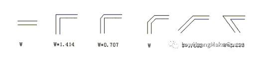
Corner line width changes for different angles
Right-angle routing has three main effects on signals: first, the corner can be equivalent to a capacitive load on the transmission line, slowing down the rise time; second, impedance discontinuity will cause signal reflection; third, EMI generated by the right-angle tip.
The parasitic capacitance caused by the right angle of the transmission line can be calculated by the following empirical formula:
C=61W(Er)[size=1]1/2[/size]/Z0
In the above formula, C refers to the equivalent capacitance of the corner (unit: pF), W refers to the width of the routing (unit: inch), εr refers to the dielectric constant of the medium, and Z0 is the characteristic impedance of the transmission line. For example, for a 4Mils 50-ohm transmission line (εr is 4.3), the capacitance caused by a right angle is about 0.0101pF, and the rise time change caused by this can be estimated:
T10-90%=2.2CZ0/2 = 2.20.010150/2 = 0.556ps
Through calculation, it can be seen that the capacitance effect caused by right-angle routing is extremely small.
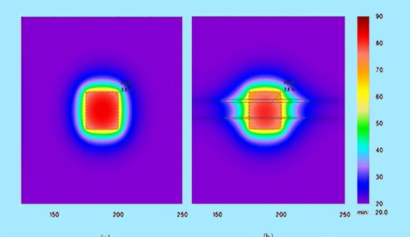
As the line width of the right-angle routing increases, the impedance at this point will decrease, so a certain signal reflection phenomenon will occur. We can calculate the equivalent impedance after the line width increases according to the impedance calculation formula mentioned in the transmission line chapter, and then calculate the reflection coefficient according to the empirical formula: ρ=(Zs-Z0)/(Zs+Z0). Generally, the impedance change caused by right-angle routing is between 7%-20%, so the maximum reflection coefficient is about 0.1. Moreover, as can be seen from the figure below, the impedance of the transmission line changes to the minimum within W/2 line length, and then returns to normal impedance after W/2 time. The entire impedance change time is extremely short, often within 10ps. Such a fast and small change is almost negligible for general signal transmission.
90-degree corner analysis
Many people have such an understanding of right-angle routing, thinking that the tip is easy to transmit or receive electromagnetic waves and generate EMI, which has become one of the reasons why many people think that right-angle routing cannot be used. However, many actual test results show that right-angle routing does not generate obvious EMI compared to straight lines. Perhaps the current instrument performance and test level restrict the accuracy of the test, but at least it shows a problem that the radiation of right-angle routing is smaller than the measurement error of the instrument itself.
In general, right-angle routing is not as terrible as imagined. At least in applications below GHz, any effects such as capacitance, reflection, EMI, etc. produced by it are almost invisible in TDR testing. High-speed PCB design engineers should focus on layout, power/ground design, routing design, vias and other aspects. Of course, although the impact of right-angle routing is not very serious, it does not mean that we can all use right-angle routing in the future. Paying attention to details is a basic quality that every excellent engineer must have. Moreover, with the rapid development of digital circuits, the signal frequency processed by PCB engineers will continue to increase. In the RF design field above 10GHz, these small right angles may become the focus of high-speed problems.
2.Differential routing
Differential signals are increasingly widely used in high-speed circuit design. The most critical signals in the circuit often use differential structure design. What makes it so popular? How can its good performance be guaranteed in PCB design? With these two questions, let’s discuss the next part.
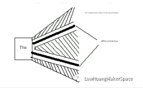
What is a differential signal? In layman’s terms, the driver sends two equal and opposite signals, and the receiver determines the logic state “0” or “1” by comparing the difference between the two voltages. The pair of traces that carry differential signals is called differential traces.
Differential signal structure diagram
Compared with ordinary single-ended signal traces, the most obvious advantages of differential signals are reflected in the following three aspects:
a. Strong anti-interference ability, because the coupling between the two differential traces is very good, when there is noise interference from the outside, it is almost coupled to the two lines at the same time, and the receiver only cares about the difference between the two signals, so the common mode noise from the outside can be completely offset.
b. Can effectively suppress EMI. For the same reason, because the polarities of the two signals are opposite, the electromagnetic fields they radiate can offset each other. The tighter the coupling, the less electromagnetic energy is released to the outside.
c. Accurate timing positioning. Since the switching change of the differential signal is located at the intersection of the two signals, unlike the ordinary single-ended signal that relies on the high and low threshold voltages for judgment, it is less affected by the process and temperature, can reduce the timing error, and is also more suitable for circuits with low amplitude signals. The currently popular LVDS (low voltage differential signaling) refers to this small amplitude differential signal technology.
For PCB engineers, the most important concern is how to ensure that these advantages of differential routing can be fully utilized in actual routing. Perhaps anyone who has been exposed to Layout will understand the general requirements of differential routing, that is, “equal length and equal distance”. Equal length is to ensure that the two differential signals always maintain opposite polarity and reduce common mode components; equal distance is mainly to ensure that the differential impedance of the two is consistent and reduce reflections. “The principle of being as close as possible” is sometimes also one of the requirements for differential routing. But all these rules are not used to copy and paste, and many engineers do not seem to understand the essence of high-speed differential signal transmission. The following focuses on several common misunderstandings in PCB differential signal design.
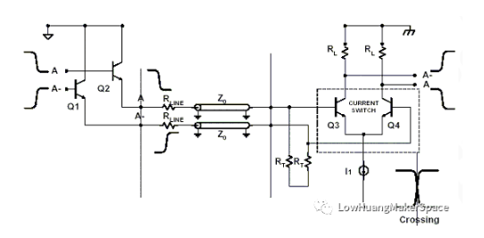
Misconception 1: It is believed that differential signals do not need a ground plane as a return path, or that differential traces provide return paths for each other. The reason for this misunderstanding is that people are confused by surface phenomena or do not have a deep enough understanding of the mechanism of high-speed signal transmission. From the structure of the receiving end in Figure 1-8-15, it can be seen that the emitter currents of transistors Q3 and Q4 are equal and opposite, and their currents at the ground just cancel each other out (I1=0), so the differential circuit is insensitive to noise signals such as ground bounce and other noise signals that may exist on the power supply and ground plane. The partial return cancellation of the ground plane does not mean that the differential circuit does not use the reference plane as the signal return path. In fact, in signal return analysis, the mechanism of differential traces and ordinary single-ended traces is the same, that is, high-frequency signals always return along the loop with the smallest inductance. The biggest difference is that in addition to coupling to the ground, differential lines also have mutual coupling. The one with stronger coupling becomes the main return path. Figure 1-8-16 is a schematic diagram of the geomagnetic field distribution of single-ended and differential signals.
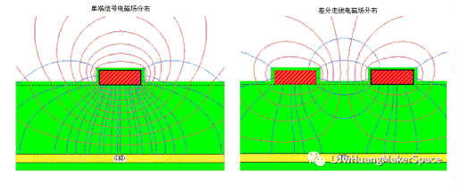
Schematic diagram of geomagnetic field distribution of single-ended signal and differential signal
In PCB circuit design, the coupling between differential traces is generally small, often accounting for only 10~20% of the coupling degree, and more is the coupling to the ground, so the main return path of the differential trace still exists in the ground plane. When the ground plane is discontinuous, the coupling between differential traces in the area without reference plane will provide the main return path, as shown in Figure 1-8-17. Although the impact of the discontinuity of the reference plane on the differential trace is not as serious as that on the ordinary single-ended trace, it will still reduce the quality of the differential signal and increase EMI, so it should be avoided as much as possible. Some designers also believe that the reference plane under the differential trace can be removed to suppress some common-mode signals in differential transmission, but theoretically this approach is not advisable. How to control the impedance? Not providing a ground impedance loop for the common-mode signal will inevitably cause EMI radiation, which is more harmful than beneficial.
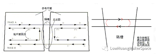
Differential signal return on discontinuous ground plane
Misconception 2: It is believed that maintaining equal spacing is more important than matching line length. In actual PCB wiring, the requirements of differential design cannot be met at the same time. Due to factors such as pin distribution, vias, and routing space, appropriate winding must be used to achieve the purpose of line length matching, but the result is that some areas of the differential pair cannot be parallel. How should we choose at this time? Before drawing a conclusion, let’s take a look at the following simulation result.
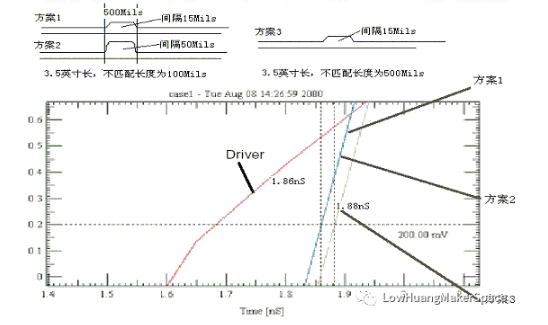
The impact of unequal spacing and mismatched line length of differential routing
From the above simulation results, the waveforms of scheme 1 and scheme 2 are almost overlapping, that is, the impact caused by unequal spacing is negligible. In comparison, the impact of mismatched line length on timing is much greater (Scheme 3). From a theoretical analysis, although inconsistent spacing will cause changes in differential impedance, the impedance change range is also very small because the coupling between differential pairs is not significant, usually within 10%, which is equivalent to the reflection caused by a via, which will not have a significant impact on signal transmission. Once the line length is mismatched, in addition to the timing offset, common mode components are introduced into the differential signal, reducing the signal quality and increasing EMI.
It can be said that the most important rule in the design of PCB differential routing is to match the line length, and other rules can be flexibly handled according to design requirements and practical applications.
Misunderstanding 3: It is believed that differential routing must be very close. Bringing differential routing close is nothing more than enhancing their coupling, which can not only improve immunity to noise, but also make full use of the opposite polarity of the magnetic field to offset the electromagnetic interference to the outside world. Although this approach is very beneficial in most cases, it is not absolute. If we can ensure that they are fully shielded and not interfered by the outside world, then we don’t need to achieve the purpose of anti-interference and EMI suppression through strong coupling with each other. How can we ensure that differential traces have good isolation and shielding? Increasing the spacing with other signal traces is one of the most basic ways. The electromagnetic field energy decreases in a square relationship with the distance. Generally, when the line spacing exceeds 4 times the line width, the interference between them is extremely weak and can be basically ignored. In addition, the isolation through the ground plane can also play a good shielding role. This structure is often used in high-frequency (above 10G) IC package PCB design. It is called CPW structure, which can ensure strict differential impedance control (2Z0), as shown in Figure 1-8-19.
CPM structure in package
Differential traces can also be routed in different signal layers, but this method is generally not recommended because the differences in impedance and vias generated by different layers will destroy the effect of differential mode transmission and introduce common mode noise. In addition, if the coupling between two adjacent layers is not tight enough, the ability of the differential routing to resist noise will be reduced, but if the appropriate spacing with the surrounding routing can be maintained, crosstalk will not be a problem. At general frequencies (below GHz), EMI will not be a serious problem. Experiments show that the radiation energy attenuation of differential routing 500 Mils apart has reached 60 dB at 3 meters, which is enough to meet the FCC’s electromagnetic radiation standards, so designers do not have to worry too much about electromagnetic incompatibility caused by insufficient coupling of differential lines.
3.Serpentine line
Serpentine line is a type of routing method often used in Layout. Its main purpose is to adjust the delay and meet the system timing design requirements. Designers must first have this understanding: serpentine lines will damage signal quality and change transmission delay, and should be avoided as much as possible during wiring. However, in actual design, in order to ensure that the signal has enough hold time, or to reduce the time offset between the same group of signals, it is often necessary to deliberately wind the line.

Several serpentine routing structures
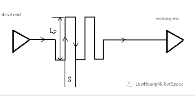
Serpentine routing model
So, what is the impact of serpentine routing on signal transmission? What should be paid attention to when routing? The two most critical parameters are the parallel coupling length (Lp) and the coupling distance (S), as shown in Figure 1-8-21. Obviously, when the signal is transmitted on the serpentine routing, coupling will occur between the parallel segments in the form of differential mode. The smaller S and the larger Lp, the greater the degree of coupling. It may cause a decrease in transmission delay and greatly reduce the quality of the signal due to crosstalk. The mechanism can refer to the analysis of common mode and differential mode crosstalk in Chapter 3.
The following are some suggestions for layout engineers when dealing with serpentine routing:
- Try to increase the distance (S) of parallel segments to at least 3H, where H refers to the distance from the signal line to the reference plane. In layman’s terms, it means routing around a large bend. As long as S is large enough, the mutual coupling effect can be almost completely avoided.
- Reduce the coupling length Lp. When the delay of twice the Lp approaches or exceeds the signal rise time, the crosstalk generated will reach saturation.
- The signal transmission delay caused by the serpentine line of the stripline or embedded microstrip is smaller than that of the microstrip. In theory, the stripline will not affect the transmission rate due to differential mode crosstalk.
- For high-speed signal lines and signal lines with strict timing requirements, try not to use serpentine lines, especially not to meander in a small range,Routing.
- You can often use serpentine routing at any angle, such as the C structure in Figure 1-8-20, which can effectively reduce mutual coupling.
- In high-speed PCB design, serpentine routing has no so-called filtering or anti-interference ability, and can only reduce signal quality, so it is only used for timing matching and has no other purpose.
- Sometimes you can consider winding in the form of spiral routing. Simulation shows that its effect is better than normal serpentine routing.
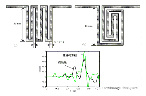
Comparison between spiral routing and ordinary serpentine routing