Scalable High Volume PCB Manufacturing Best Practices
Key Takeaways
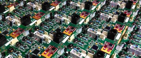
When scaling PCB manufacturing operations to 1,000+ units, prioritizing process standardization and DFM (Design for Manufacturing) protocols ensures consistency across batches. You’ll want to align with PCB manufacturing companies that offer automated panelization and material optimization to reduce PCB manufacturing cost while maintaining quality.
“Adopting a modular design approach early in prototyping accelerates the transition to mass production by 30–40%,” notes a senior engineer at a Tier-1 PCB manufacturing business.
Critical considerations include:
- Automated testing integration to maintain defect rates below 0.5%
- Thermal management enhancements for high-density boards
- Supplier partnerships for bulk material procurement
| Traditional Approach | Scalable Strategy |
|---|---|
| Manual quality checks | In-line AOI (Automated Optical Inspection) |
| Single-source suppliers | Multi-vendor material networks |
| Fixed panel sizes | Dynamic panelization algorithms |
To minimize PCB manufacturing cost, prioritize standardized component libraries and avoid over-engineering. Partnering with PCB manufacturing companies that offer volume-tiered pricing ensures cost predictability. Finally, implement real-time yield monitoring to identify bottlenecks before they impact deadlines.

High-Volume PCB Production Thresholds Explained
When scaling PCB manufacturing operations beyond 1,000+ units, you’ll encounter critical thresholds that separate successful mass production from costly bottlenecks. First, minimum order quantities (MOQs) often dictate feasibility—many PCB manufacturing companies require commitments that align with their production line capacities. This demands precise forecasting to avoid overstocking or shortages. Second, equipment specialization becomes non-negotiable: high-speed pick-and-place machines, automated optical inspection (AOI), and advanced soldering systems ensure consistency at scale.
Balancing PCB manufacturing cost with quality requires optimizing material selection and layer stacking early in the design phase. For instance, using standardized panel sizes reduces waste, while adhering to design for manufacturability (https://www.andwinpcba.com), to identify failure points before full-scale runs.
Finally, selecting partners for your PCB manufacturing business means prioritizing facilities with proven scalability. Look for certifications like ISO 9001 and IPC-A-610 to ensure they meet reliability benchmarks. By evaluating these thresholds systematically, you avoid the pitfalls of underprepared transitions and maintain profitability as demand grows.
DFM Optimization for Scalable PCB Manufacturing
To achieve scalability in PCB manufacturing, you need to prioritize design for manufacturability (DFM) principles from the earliest stages. This means aligning your board layouts with the technical capabilities of PCB manufacturing companies while balancing PCB manufacturing cost constraints. Start by standardizing component footprints and minimizing complex geometries—features like ultra-fine traces or non-standard via sizes increase production risks at scale.
Collaborate with your fabrication partner during design reviews to identify potential bottlenecks, such as solder mask alignment tolerances or copper balancing requirements. Automated DFM analysis tools can flag issues like insufficient spacing for high-speed pick-and-place machines, ensuring designs meet volume-ready specifications. For instance, optimizing panel utilization by nesting multiple boards reduces material waste, directly lowering PCB manufacturing business expenses.
Additionally, consider thermal management and material selection early. High-volume runs demand designs that perform consistently across temperature variations, avoiding rework costs. By embedding DFM checks into your workflow, you create a seamless bridge between prototyping and mass production, ensuring reliability while maintaining competitive per-unit pricing. This proactive approach not only accelerates time-to-market but builds a foundation for scaling without compromising quality.
Cost Efficiency Unit PCB Production
Achieving cost efficiency in PCB manufacturing requires balancing economies of scale with precision engineering. When producing 1,000+ units, material utilization and process standardization become critical levers. Leading PCB manufacturing companies optimize panelization layouts to minimize substrate waste, often reducing raw material expenses by 12–18% per batch. Simultaneously, implementing design-for-manufacturability (DFM) checks early ensures designs align with production capabilities, avoiding costly rework during scaling.
Your choice of fabrication technologies directly impacts PCB manufacturing cost. For example, selecting laser-drilled microvias over mechanical drilling cuts processing time by 30% in multilayer boards, while automated optical inspection (AOI) systems reduce defect rates below 0.5%. Partnering with PCB manufacturing business partners that offer volume-tiered pricing models further lowers per-unit expenses without compromising quality.
To sustain efficiency, analyze cycle time metrics across prototyping and mass production phases. Streamlining workflows—like synchronizing solder mask application with surface finishes—can trim lead times by 20%. Finally, negotiate component procurement agreements aligned with your production forecasts; bulk purchasing of FR-4 substrates or high-frequency laminates often yields 15–25% savings. These strategies ensure your high-volume operations remain agile and economically viable as demand fluctuates.

Prototype-to-Mass Production Transition Strategies
Successfully scaling from prototype to high-volume PCB manufacturing requires strategic alignment between design intent and production realities. Start by validating your prototype against design-for-manufacturability (DFM) guidelines to identify potential bottlenecks in materials, layer stack-ups, or component placement. Collaborate early with PCB manufacturing companies to ensure your design aligns with their equipment capabilities and tolerances, minimizing costly revisions later.
Implement phased testing to bridge the gap between low-volume and mass production. For instance, pilot runs of 100–500 units can reveal inconsistencies in solder paste application or thermal management that prototypes might miss. Use this data to refine processes like automated optical inspection (AOI) settings or panelization layouts before committing to 1,000+ unit batches.
Cost control becomes critical at scale. Optimize PCB manufacturing cost by standardizing materials, negotiating bulk pricing for substrates, and reducing setup cycles through panel optimization. Consider modular tooling designs that allow flexible adjustments for future design iterations without halting production lines.
Finally, establish clear communication channels with your PCB manufacturing business partners. Shared dashboards for real-time yield tracking and failure analysis ensure rapid response to quality deviations. This collaborative approach minimizes downtime and maintains consistency across high-volume orders, enabling seamless transitions while preserving reliability.
Advanced Process Optimization for Reliability
To achieve consistent reliability in high-volume PCB manufacturing, you must prioritize process-driven quality controls that address variability at scale. Start by implementing automated optical inspection (AOI) systems paired with real-time data analytics to detect micron-level deviations in trace widths or solder mask alignment. Leading PCB manufacturing companies now integrate thermal stress testing into production cycles, simulating 5+ years of operational wear within controlled environments to validate board durability.
Optimizing PCB manufacturing cost without compromising reliability requires balancing material selection with process efficiency. For instance, using laser-direct imaging (LDI) reduces photolithography errors by 30%, minimizing rework rates in batches exceeding 1,000 units. Concurrently, adopt statistical process control (SPC) protocols to monitor critical parameters like copper plating thickness, ensuring ±2% tolerance compliance across all layers.
For businesses scaling a PCB manufacturing business, invest in closed-loop feedback systems that correlate test results with design adjustments. This approach not only streamlines failure root-cause analysis but also strengthens traceability—a non-negotiable for aerospace or medical applications. By embedding these optimizations early, you create a repeatable framework that scales reliability alongside production volume.
Selecting High-Capacity PCB Assembly Partners
When scaling PCB manufacturing operations, choosing the right assembly partner becomes critical to maintaining quality and meeting deadlines. High-volume production demands partners with proven expertise in PCB manufacturing business dynamics, including advanced equipment, material sourcing networks, and workforce scalability. Start by verifying certifications like ISO 9001 and IPC-A-610 to ensure adherence to industry standards.
Evaluate their capacity for high-volume PCB manufacturing by auditing facilities for automated pick-and-place systems, reflow soldering lines, and throughput rates that align with your project’s scale. Prioritize PCB manufacturing companies with transparent PCB manufacturing cost structures, as hidden fees can derail budgets at scale. Ask about their design-for-manufacturability (DFM) review processes—rigorous DFM protocols minimize redesigns and delays during mass production.
Look for partners offering seamless integration between prototyping and full-scale runs, as this reduces transition friction. Confirm their quality control frameworks, such as automated optical inspection (AOI) and X-ray testing, which are non-negotiable for maintaining reliability in bulk orders. Finally, assess their supply chain resilience—vendors with diversified material sources mitigate risks of component shortages, ensuring uninterrupted PCB manufacturing workflows.
Quality Control in Bulk PCB Manufacturing
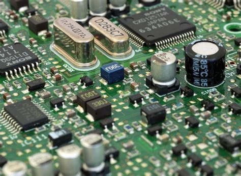
When scaling PCB manufacturing to high volumes, maintaining consistent quality becomes both a technical challenge and a business imperative. Defect rates that seem negligible in small batches can escalate rapidly in 1,000+ unit runs, directly impacting PCB manufacturing cost and end-product reliability. Leading PCB manufacturing companies implement multi-layered inspection systems, combining automated optical inspection (AOI) for surface defects with X-ray verification of internal layers and solder joints. You’ll want to integrate design-for-manufacturability (DFM) checks at every stage—from material selection to final testing—to prevent costly rework.
Statistical process control (SPC) tools track critical parameters like copper thickness and dielectric consistency, flagging deviations before they cascade into systemic failures. For PCB manufacturing business models prioritizing scalability, pairing these systems with real-time data analytics ensures traceability across batches. Remember: even minor improvements in first-pass yield—achieved through rigorous process validation—compound into significant savings at volume. Partnering with certified suppliers for materials and components further reduces variability, while periodic third-party audits help maintain compliance with industry standards like IPC-A-600. Ultimately, balancing stringent quality protocols with production throughput requires both technological investment and cross-functional coordination between engineering and manufacturing teams.
Automated Testing for Scalability Maintenance
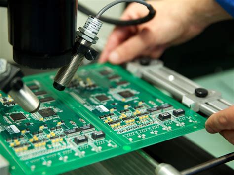
To maintain PCB manufacturing scalability without compromising quality, automated testing frameworks become indispensable. By implementing in-circuit testing (ICT) and automated optical inspection (AOI) systems, you ensure rapid defect detection across thousands of units while minimizing human error. These systems integrate with PCB manufacturing companies’ existing production lines, enabling real-time data analysis to identify process bottlenecks or recurring faults. For example, AOI cameras can scan 20,000+ solder joints per hour, flagging inconsistencies that might escalate into costly rework during mass production.
Transitioning from prototype to high-volume runs demands testing protocols that scale proportionally. Design-for-manufacturability (DFM) principles should align with automated test parameters, ensuring boards are optimized for both production efficiency and testability. This reduces PCB manufacturing cost by catching issues early—before they compound across batches. Advanced PCB manufacturing business models leverage machine learning algorithms to predict failure patterns, further refining testing accuracy over time.
However, balancing speed and precision requires strategic investment. While initial setup costs for automated systems may seem high, they offset long-term expenses tied to manual inspections or recalls. Partnering with PCB manufacturing companies that prioritize scalable testing infrastructure ensures your operations remain agile as demand fluctuates—a critical advantage in competitive electronics markets.
Conclusion
When scaling PCB manufacturing operations to meet high-volume demands, success hinges on balancing reliability, cost efficiency, and process adaptability. By implementing DFM protocols early and partnering with experienced PCB manufacturing companies, you reduce risks of delays or defects that escalate PCB manufacturing cost over time. Automated testing systems and rigorous quality checks ensure consistency across thousands of units, while advanced process optimizations—like panelization and material standardization—streamline workflows without compromising performance.
Transitioning from prototypes to mass production requires aligning design intent with manufacturing realities. Iterative prototyping paired with feedback from PCB manufacturing business experts helps refine designs for scalability. Additionally, selecting high-capacity partners with proven track records in PCB manufacturing ensures access to technologies like laser drilling or HDI processes, critical for maintaining precision at scale.
Ultimately, achieving sustainable growth in high-volume PCB manufacturing demands a holistic approach—integrating design foresight, process innovation, and collaborative partnerships. By prioritizing these strategies, you position your operations to meet rising demands while controlling costs and upholding quality standards.
Frequently Asked Questions
How do PCB manufacturing companies ensure scalability for 1,000+ unit orders?
They implement design-for-manufacturing (DFM) protocols early in development, optimize panelization layouts, and use automated assembly lines. Rigorous material selection and standardized testing procedures ensure repeatable quality across batches while controlling PCB manufacturing cost.
What factors most impact PCB manufacturing cost in high-volume production?
Key drivers include raw material quality, layer count, surface finishes, and tolerances. Bulk material procurement, reduced setup cycles via automation, and minimizing scrap rates through process optimization lower per-unit costs. Partnering with PCB manufacturing businesses that offer tiered pricing models improves cost predictability.
Why partner with specialized PCB manufacturing businesses for 1,000+ unit projects?
Established providers combine advanced equipment (e.g., SMT lines, AOI systems) with expertise in scalable PCB manufacturing. They streamline prototyping-to-mass-production transitions by resolving design flaws early, ensuring supply chain resilience, and maintaining traceability for compliance.
How is quality control maintained in high-volume PCB manufacturing?
Automated optical inspection (AOI), in-circuit testing (ICT), and functional testing protocols are applied at multiple stages. Statistical process control (SPC) monitors production metrics in real time, while ISO-certified workflows ensure defect rates below 0.1% even at scale.
Ready to Optimize Your High-Volume PCB Production?
For tailored solutions that align with your PCB manufacturing goals, please click here to consult experts specializing in scalable, cost-efficient production workflows.