Several issues to consider when designing PCBs
With the vigorous development of the PCB industry, more and more engineering and technical personnel have joined the design and manufacture of PCBs. However, since PCB manufacturing involves many fields and a considerable number of PCB
design engineers (Layout personnel) have not engaged in or participated in the production and manufacturing process of PCBs, the design process focuses on electrical performance and product functions.
However, when downstream PCB processing plants receive orders and in the actual production process, there are many problems that are not considered in the design, which cause product processing difficulties, extended processing cycles or product hidden dangers.
The following points are analyzed for such problems that are not conducive to processing and production, for reference by PCB design and production engineers:
For ease of expression, the analysis is conducted from seven aspects: cutting, drilling, circuits, solder mask, characters, surface treatment and forming:
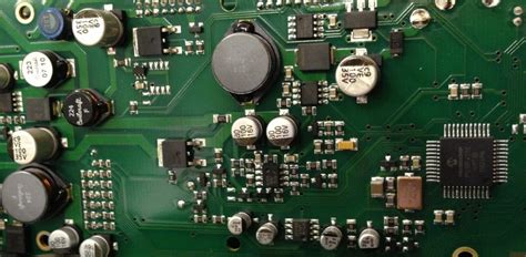
I. The main considerations for cutting are the thickness of the board and the thickness of the copper:
For boards with a thickness greater than 0.8MM, the standard series is: 1.0 1.2 1.6 2.0 3.2 MM. Boards with a thickness less than 0.8MM are not considered standard series. The thickness can be determined according to needs
, but the commonly used thicknesses are: 0.1 0.15 0.2 0.3 0.4 0.6MM. These materials are mainly used for the inner layer of multilayer boards.
When designing the outer layer, pay attention to the selection of board thickness. The production and processing requires the increase of copper plating thickness, solder mask thickness, surface treatment (tin spraying, gold plating, etc.) thickness, and character, carbon oil, etc. The actual
production of sheet metal will be 0.05-0.1MM thicker, and the tin plate will be 0.075-0.15MM thicker. For example, when the finished product requires a thickness of 2.0 mm, when a 2.0 mm plate is normally selected for cutting, the finished product thickness will reach between 2.1-2.3 mm, taking into account the plate tolerance and processing tolerance.
If the design requires that the finished product thickness cannot be greater than 2.0 mm, the plate should be selected as a 1.9 mm non-conventional plate. The PCB processing plant needs to temporarily order from the plate manufacturer, and the delivery cycle will become very long. When the inner layer is made, the thickness after lamination can be adjusted by the thickness and structural configuration of the semi-cured sheet (PP), and the selection range of the core board can be more flexible.
For example, if the finished product thickness requires 1.6 mm, the plate (core board) can be 1.2 mm or 1.0 mm.
As long as the thickness of the laminated plate is controlled within a certain range, the finished product thickness requirement can be met. Another issue is the plate thickness tolerance. PCB designers should consider the plate thickness tolerance after PCB processing while considering the product assembly tolerance. There are three main aspects that affect the finished product tolerance: plate material tolerance, lamination tolerance, and outer layer thickening tolerance. Several conventional board tolerances are provided for reference: (0.8-1.0)±0.1 (1.2-1.6)±0.13 2.0±0.18
3.0±0.23 The lamination tolerance is controlled between ±(0.05-0.1)MM according to the number of layers and board thickness.
In particular, for boards with board edge connectors (such as printed plugs), the board thickness and tolerance need to be determined according to the requirements of matching with the connector.
The problem of surface copper thickness, since the hole copper needs to be completed by chemical copper deposition and electroplating,
if no special treatment is done, the surface copper thickness will be thickened when the hole copper is thickened. According to the IPC-A-600G standard, the minimum copper plating thickness is 20um for levels 1 and 2, and 25um for level 3. Therefore, when making circuit boards, if the copper thickness requires 1OZ (minimum 30.9um), the material will sometimes be cut according to the line width/line spacing. HOZ (minimum 15.4um) is selected. Excluding the allowable tolerance of 2-3um, the minimum can reach 33.4um. If 1OZ is selected, the minimum copper thickness of the finished product will reach 47.9um. Other copper thickness calculations can be deduced in the same way.
II. Drilling mainly considers the tolerance of the aperture size, the pre-enlargement of the drill hole, the processing of the hole to the edge of the board, the non-metallized hole, and the design of the positioning hole:
Currently, the smallest processing drill for mechanical drilling is 0.2mm, but due to the thickness of the hole wall copper and the thickness of the protective layer, the design aperture needs to be enlarged during production. The tin-spraying plate needs to be enlarged by 0.15mm
The gold plate needs to be enlarged by 0.1mm.
The key issue here is, if the aperture is enlarged, does the distance from such holes to the circuit and copper skin meet the processing requirements? Is the solder ring of the originally designed circuit pad
enough? For example, when designing, the via hole diameter is 0.2mm, and the pad diameter is 0.35mm. Theoretical calculations show that the solder ring can be processed with a single side of 0.075mm, but when the drill bit is enlarged according to the tin plate, there is no solder ring. If the pad cannot be enlarged due to spacing problems, the board cannot be processed.
Aperture tolerance problem: At present, most domestic drilling machines have a drilling tolerance of ±0.05mm. In addition to the tolerance of the plating thickness in the hole, the metallized hole tolerance is controlled at ±0.075mm, and the non-metallized hole tolerance is controlled at ±0.05mm.
Another problem that is easily overlooked is the isolation distance from the drilling hole to the inner copper skin or wire of the multilayer board.
Since the drilling positioning tolerance is ±0.075mm, the expansion and contraction deformation of the graphics after the inner laminate during lamination has a tolerance change of ±0.1mm. Therefore, when designing, the distance from the hole edge to the wire or copper foil must be guaranteed to be more than 0.15mm for 4-layer boards, and more than 0.2mm for 6-layer or 8-layer boards to facilitate production.
There are three common ways to make non-metallized holes: dry film sealing or plastic plugging, so that the copper plated in the hole can be removed from the hole wall copper layer during etching because there is no corrosion protection. Note that for dry film sealing, the hole diameter cannot be greater than 6.0mm, and for plastic plugging, the hole diameter cannot be less than 11.5mm. Another way is to use secondary drilling to make non-metallized holes. Regardless of the method used, there must be no copper foil within 0.2mm around the non-metallized hole.
The design of positioning holes is often an issue that is easily overlooked.
During the processing of circuit boards, testing, external punching or electric milling all require holes larger than 1.5mm as positioning holes for board fixation. When designing, it is necessary to consider distributing the holes in a triangle as much as possible on the three corners of the circuit board.
Three. The main consideration for circuit production is the impact of circuit etching.
Due to the impact of side etching, the copper thickness and different processing techniques are considered during production and processing. The circuit needs to be pre-roughened to a certain extent. The conventional compensation for HOZ copper of tin-spraying and gold-immersion board is 0.025mm, and the conventional compensation for 1OZ copper thickness is 0.05-0.075mm. The conventional line width/line spacing production and processing capacity is 0.075/0.075mm. Therefore, when designing, when considering the maximum line width/line spacing wiring, it is necessary to consider the compensation problem during production. Since the gold-plated board does not need to remove the gold-plated layer on the circuit after etching, the line width does not decrease, so no compensation is required. However, it should be noted that since side etching still exists, the copper line width under the gold layer will be smaller than the gold layer line width. If the copper thickness is too thick or the etching is excessive, it is very easy to cause the gold surface to collapse, resulting in poor welding. For lines with characteristic impedance requirements, the line width/line spacing requirements will be more stringent. 4. The most troublesome part of solder mask production is the solder mask treatment on the via hole:
Because the via hole has the function of conducting electricity, many PCB design engineers will design it as a finished product online test point after assembling components, and even a few will design it as a component plug-in hole.
In the design of conventional via holes, in order to prevent tin from sticking during welding, it will be designed as a cover oil. If it is a test point or plug-in hole, a window must be opened.
However, the cover oil of the via hole of the spray tin plate is very easy to cause tin beads to be hidden in the hole, so a considerable number of products are designed as via oil plugging, and the BGA position is also treated as oil plugging for the convenience of packaging. However, when the aperture is larger than 0.6mm, it will increase the difficulty of plugging oil (not fully plugged), so there are also tin spray plates designed to open a semi-open window with a single side larger than the aperture by 0.065mm, and tin is sprayed within the range of 0.065mm on the hole wall and the hole edge.
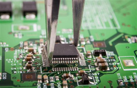
V. When processing characters, the main consideration is the addition of pads and related markings on the characters.
As the layout of components becomes denser and denser, and the characters should not be printed on the pads, at least the distance from the characters to the pads should be more than 0.15mm, the component frame and component symbol sometimes cannot be completely distributed on the circuit board. Fortunately, most of the patches are now completed by machines. Therefore, if it is really impossible to adjust during design, you can consider printing only the character frame and not the component symbol.
The common contents added by the mark include supplier logo, UL certification logo, flame retardant grade, anti-static mark, production cycle, customer-specified logo, etc. The meaning of each logo must be clarified, and it is best to reserve and specify the location for adding.
Six. The impact of PCB surface coating (plating) on design:
The conventional surface treatment methods that are widely used at present are OSP gold plating, immersion gold, and tin spraying. We can compare their advantages and disadvantages from the aspects of cost, solderability, wear resistance, oxidation resistance, different production processes, drilling and circuit modification.
OSP process: low cost, good conductivity and flatness, but poor oxidation resistance, not conducive to preservation.
The drilling compensation is usually made according to 0.1mm, and the HOZ copper thickness line width compensation is 0.025mm. Considering that it is very easy to oxidize and be contaminated with dust, the OSP process is completed after forming and cleaning. When the size of a single piece is less than 80MM, it must be considered to be delivered in the form of spliced pieces. Electroplating nickel gold process: good oxidation resistance and wear resistance. When used for plugs or contact points, the thickness of the gold layer is greater than or equal to 1.3um. The thickness of the gold layer used for welding is usually 0.05-0.1um, but the relative solderability is poor. The drilling compensation is made according to 0.1mm, and the line width is not compensated. Note that when making gold plates with a copper thickness of more than 1OZ, the copper layer under the surface gold layer is very likely to cause excessive etching and collapse, causing solderability problems.
Because gold plating requires current assistance, the gold plating process is designed before etching.
While the complete surface treatment also plays the role of corrosion resistance, the process of removing corrosion resistance is reduced after etching, which is also the reason why the line width is not compensated. Chemical nickel-gold plating (immersion gold) process: good oxidation resistance and toughness, flat coating, widely used in SMT boards, drilling compensation is made according to 0.15mm, HOZ copper thickness line width compensation is 0.025mm,
Because the immersion gold process is designed after solder mask, corrosion resistance protection needs to be used before etching, and corrosion resistance needs to be removed after etching, so the line width compensation is more than gold-plated boards, so immersion gold is applied after solder mask,
Most circuits are covered with solder mask and do not need immersion gold.
Compared with boards with large areas of copper, the amount of gold salt consumed by immersion gold boards is significantly lower than that of gold-plated boards.
Spray tin board (63 tin/37 lead) process: oxidation resistance and toughness are relatively good, flatness is poor, drilling compensation is made according to 0.15mm, HOZ copper thickness line width compensation is 0.025mm, process
Basically the same as immersion gold, currently the most common surface treatment method.
Since the EU proposed the ROHS directive, refusing to use six harmful substances including lead, mercury, cadmium, hexavalent chromium, polybrominated diphenyl ether (PBDE) and polybrominated biphenyl (PBB), surface treatment introduced new processes such as pure tin spraying (tin copper ), pure tin spraying (tin silver copper), immersion silver and immersion tin to replace the lead tin spraying process.
Seven. Board assembly, appearance production is also a difficult problem to consider comprehensively during design:
The board assembly must first consider the ease of processing. When milling the appearance, the distance should be based on a milling cutter diameter (usually 1.6 1.2 1.0 0.8) to assemble the board. When punching the board appearance, pay attention to whether the distance from the hole and line to the board edge is greater than one board thickness, and the minimum punching slot size must be greater than 0.8mm. If V-CUT is used for connection, the board edge line and copper skin must be guaranteed to be 0.3mm away from the center of the V-CUT.


