Signal Return Path and Cross-Talk in High-Speed PCB Design
Abstract
This paper explores two critical aspects of high-speed printed circuit board (PCB) design: signal return current paths and the challenges posed by plane splits or cross-segmentation. As digital systems continue to operate at higher frequencies with faster edge rates, proper management of signal return paths becomes essential for maintaining signal integrity, minimizing electromagnetic interference (EMI), and ensuring reliable system operation. The discussion covers fundamental concepts, analysis techniques, and practical design solutions for handling return current paths and mitigating issues caused by reference plane discontinuities in modern high-speed PCB designs.
1. Introduction
In the realm of high-speed digital design, where clock frequencies routinely exceed several gigahertz and signal rise times measure in picoseconds, PCB layout considerations extend far beyond simple connectivity. Two particularly challenging aspects that demand careful attention are:
- The management of signal return current paths
- The effects of plane splits or segmentation on signal integrity
These factors significantly influence key performance metrics including signal quality, power distribution network (PDN) impedance, and radiated emissions. Failure to properly address these concerns can lead to intermittent failures, signal integrity issues, and EMI compliance problems that often prove difficult to diagnose and rectify in later design stages.
2. Fundamentals of Signal Return Currents
2.1 The Concept of Return Current Path
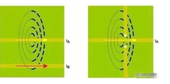
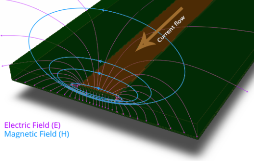
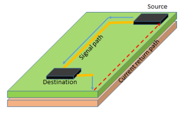
Contrary to common intuition, high-frequency signals do not simply travel along the trace from driver to receiver. At high frequencies, current flows in closed loops, and the return current seeks the path of least impedance (not just resistance) back to its source. For frequencies above approximately 1 MHz, this path typically lies directly beneath the signal trace in the adjacent reference plane.
2.2 Skin Effect and Current Distribution
The skin effect causes high-frequency currents to concentrate near the surface of conductors. In PCB interconnects:
- At 1 GHz, current penetrates only about 2.1 μm into copper
- Return currents distribute within about 3-5 times the dielectric thickness below the trace
- This concentration increases the effective resistance at high frequencies
2.3 Reference Planes and Their Role
Reference planes serve multiple critical functions:
- Provide low-impedance return paths for high-frequency signals
- Form controlled impedance transmission lines with signal traces
- Shield against EMI radiation and crosstalk
- Distribute power with low inductance
3. Return Current Path Analysis
3.1 DC vs. AC Return Paths
The behavior of return currents differs significantly between low and high frequencies:
DC and Low Frequencies (Below ~1 kHz):
- Current follows the path of least resistance
- Spreads widely through available conductors
- Ohmic losses dominate
High Frequencies (Above ~1 MHz):
- Current follows the path of least impedance
- Concentrates directly beneath signal traces
- Inductive effects dominate
3.2 Calculating Return Current Distribution
The return current density J(x) beneath a microstrip trace can be approximated by:
J(x) = (I₀ / πh) * (1 / (1 + (x/h)²))
Where:
- I₀ = total signal current
- h = dielectric thickness between trace and plane
- x = lateral distance from trace centerline
This distribution shows that 80% of the return current flows within ±h of the trace centerline.
3.3 Impedance Considerations
The loop inductance Lₗₒₒₚ of a trace and its return path is given by:
Lₗₒₒₚ ≈ (μ₀ / π) * ln(5h/w)
Where:
- μ₀ = permeability of free space (4π × 10⁻⁷ H/m)
- w = trace width
This demonstrates why keeping h small reduces loop inductance and improves signal integrity.
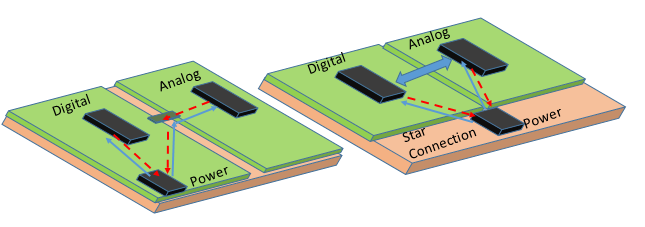
4. Plane Splits and Cross-Segmentation
4.1 Definition and Common Causes
Plane splits occur when:
- Mixed-signal designs require separate analog and digital grounds
- Multiple power domains exist on the same layer
- Board partitioning creates isolated regions
- Design constraints prevent continuous planes
4.2 Problems Created by Plane Splits
When a signal trace crosses a plane split:
- The return current path is disrupted
- The transmission line characteristics change abruptly
- Significant impedance discontinuities occur
- Common-mode currents may develop
- Radiated emissions increase
4.3 Quantifying the Impact
The impedance discontinuity at a plane split can be modeled as:
ΔZ ≈ jωLₑₓₜ + 1/(jωCₑₓₜ)
Where Lₑₓₜ and Cₑₓₜ represent the extra loop inductance and capacitance created by the split.
5. Mitigation Strategies
5.1 Managing Return Paths
- Maintain Continuous Reference Planes: Preferably use solid planes without unnecessary splits
- Minimize Dielectric Thickness: Thinner dielectrics reduce loop inductance
- Provide Adjacent Return Vias: For layer transitions, place return vias close to signal vias
- Route Critical Signals on Layers with Solid References: Avoid routing over plane splits
5.2 Handling Necessary Plane Splits
When splits are unavoidable:
- Bridge with Capacitors: Place high-frequency capacitors (0.1μF and 0.001μF in parallel) near crossing points
- Implement “Moats and Drawbridges”: Use controlled connections between isolated regions
- Route Orthogonal to Splits: When possible, arrange traces perpendicular to split boundaries
- Use Embedded Planes: For critical signals, maintain continuous reference planes in inner layers
5.3 Advanced Techniques
- Differential Signaling: Naturally confines return currents and reduces sensitivity to plane discontinuities
- Buried Stripline Routing: Provides shielding from both sides
- Via Stitching: Creates multiple parallel return paths around splits
- 3D Field Solvers: Use simulation tools to analyze complex return path scenarios
6. Practical Design Guidelines
- Layer Stackup Planning:
- Place critical signals between solid reference planes
- Maintain symmetry to prevent warping and balance impedance
- Use multiple ground planes for complex designs
- Routing Practices:
- Avoid crossing splits for high-speed signals (>100 MHz)
- If crossing is unavoidable, provide nearby return paths
- Keep high-speed traces short and direct
- Component Placement:
- Position decoupling capacitors close to power pins
- Group components by power domain
- Consider return paths when placing connectors
- Mixed-Signal Layout:
- Implement single-point grounding for low frequencies
- Maintain plane continuity for high-frequency portions
- Use careful partitioning rather than arbitrary splits
7. Measurement and Verification
7.1 Simulation Approaches
- 2D Field Solvers: Calculate impedance and losses for simple structures
- 3D Full-wave Solvers: Analyze complex geometries and discontinuities
- Time-domain Reflectometry (TDR) Simulation: Identify impedance variations
7.2 Physical Measurement Techniques
- TDR Measurements: Reveal actual impedance profiles
- Near-field Scanning: Identifies EMI hot spots
- Vector Network Analysis: Characterizes S-parameters

8. Case Studies
8.1 DDR Memory Interface
A 2.5 Gbps DDR3 interface experienced intermittent errors. Analysis revealed:
- Data lines crossed multiple ground plane splits
- Return currents took long detours, increasing loop area
- Solution: Added stitching capacitors and rerouted critical traces
8.2 10G Ethernet PHY
A 10GbE design failed radiated emissions testing:
- Differential pairs routed over split planes
- Common-mode currents developed at split crossings
- Fix: Implemented continuous ground reference and improved symmetry
9. Future Trends and Challenges
As data rates continue increasing (56G PAM4, 112G SerDes):
- Material Properties: Become more critical at higher frequencies
- 3D Integration: Creates new return path challenges
- Power Delivery: Must accommodate faster switching currents
- Manufacturing Tolerances: Become more significant relative to wavelength
10. Conclusion
Proper management of signal return paths and careful handling of plane splits are essential for successful high-speed PCB design. By understanding the underlying physics, applying appropriate design techniques, and verifying through simulation and measurement, designers can avoid common pitfalls and achieve robust, high-performance systems. As speeds continue to increase, these considerations will only grow more critical, requiring ongoing education and adaptation of design methodologies.