Simulation of 1.6T optical module
Regarding the simulation of optical modules, we have simulated optical modules from 10GE to 1.6TE. Many customers initially wanted to see the eye diagram, but after our explanation, they finally agreed to perform passive simulation according to the protocol. Today, let’s talk about why we only simulate the passive method instead of the active method to see the eye diagram.
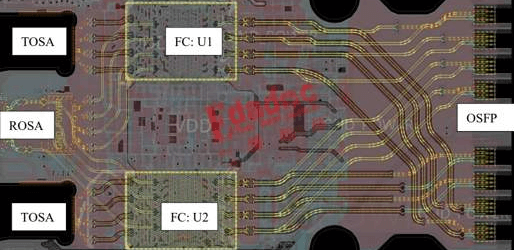
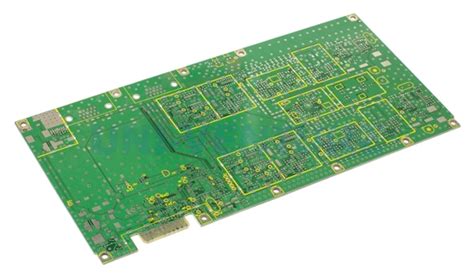
The following is a partial design circuit diagram of one of our 1.6T optical modules. These high-speed signal lines are divided into two parts: one part is from the OSFP gold finger to the middle DSP chip, which consists of 8 pairs of TX and 8 pairs of RX, each pair of 200/224Gbps constitutes the channel for sending and receiving 1.6TE; the other part is from the chip to the TOSA and ROSA interface pads, which is also composed of 8 pairs of TX and 8 pairs of RX, each pair of 200/224Gbps. There are protocol loss requirements for the gold finger to the DSP chip, and the latter part of the protocol does not define relevant electrical requirements.
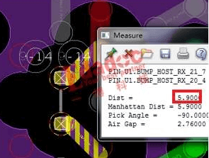
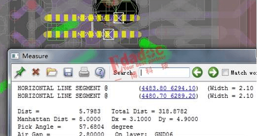
At first glance, it seems that the optical modules of 400GE and 800GE are the same routine, and it is hard to tell where the difficulty lies. However, if you look closely, the difficulty is not the same level. The main difficulty is that the pitch of the middle chip (the center spacing of the chip pad) is only 0.15mm, as shown in the figure below.
How to route the Pitch with such a small pitch?
And it is differential routing, which is very difficult and challenging for the design. The design of such a small pitch generally requires the use of mSAP process and arbitrary-order HDI design. This process is between the chip packaging substrate and the PCB board. If you are interested, you can let our brother Dong introduce it later. Today, we will skip it first. As long as we know that there is this process, we can see why we can’t use ordinary processes by looking at our routing line width. Just ask the differential line width of 2.1mil and the spacing of 2.8mil. Can ordinary PCB production process produce it?
At this time, someone may ask, the design difficulty is understandable, so what are the difficulties in simulating this 1.6T optical module?
In fact, compared with simulation, design is simple. Design only needs to ensure connectivity. In simple terms, as long as the line can be smoothly routed, half of the success is achieved. The difficulty lies in not only routing the line, but also ensuring the signal quality, which must be guaranteed by simulation. As mentioned earlier, the maximum signal rate of the 1.6TE optical module is 224Gbps, of course, it is PAM4 encoded, so its base frequency reaches 56GHz. The higher the frequency, the greater the simulation difficulty, and the subsequent line loss is also large. A little difference will affect the final performance, such as material selection, different layers of wires and via optimization methods, etc.; ordinary through-hole design does not have much difference in via characteristics when the frequency is not too high, but after 30GHz or even 50GHz, and then superimposed with arbitrary-order HDI vias, vias on different layers need to be simulated separately, and the pads at the gold finger also need special optimization. We will add a 3D model of the connector to simulate the characteristics when the connector is actually plugged in, which is closer to the actual situation and the simulation is more accurate; the consequence of all these operations is that the workload increases and more simulation time is required.
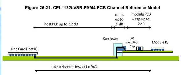
Why do many simulations of optical modules only simulate passive and rarely simulate active eye diagrams and bit error rates? This is indeed a topic of concern to many people. First, let’s take a look at the passive requirements of the optical module VSR protocol. The following figure is an excerpt from the OIF-CEI-5.1 protocol about the reference model and loss requirements of 112G-VSR-PAM4 for PCB channels.
The protocol has clear requirements for passive insertion loss.
The maximum loss on the host motherboard is 12dB, the maximum loss of the connector is 2dB, and the maximum loss of the optical module and capacitor is 2dB. The total system loss is 16dB. Generally speaking, as long as the PCB board level can meet this loss requirement, it has met the protocol indicators. The rest is the chip (it is possible that some chips have poor performance).
For simulation, in the absence of chip ami model, we only need to ensure that the loss at PCB board level meets the above protocol requirements.
Generally, the passive loss index will be more stringent. As long as the passive loss is met, of course, other indicators such as return loss, modal and crosstalk must also be met, then most chips can work normally, because the performance of the chip must also be in accordance with the protocol index requirements. Everyone must work within the framework of this protocol, and no link can be separated from this protocol framework, otherwise there will be no fun. This is the benefit of having a protocol.
Passive simulation is relatively simple.
As long as there are PCB design files, stacking and material information, modeling simulation optimization can be started. As long as the simulation method is appropriate and the material information is accurate, the results of passive simulation can be used as a basis for judgment; but active simulation will be much more complicated, requiring all the information of the system, such as the ami model of the chip on the motherboard Host and the optical module, the 3D and S parameter model of the connector, and the routing conditions on the motherboard Host and the optical module (such as S parameter model, PCB file and stacking information, etc.). Many times, if you are not a system manufacturer, you can rarely collect all these models.
For example, if you are a motherboard host manufacturer, it is difficult to get the data of the optical module manufacturer, because the motherboard host must be compatible with the optical modules of various manufacturers; and if you are an optical module manufacturer, you don’t have the data of the motherboard host, and they don’t just supply the host to a certain host, so it is difficult to do system simulation together. Now that the protocol has passive segmentation index requirements, then according to the principle of “railway workers each manage a section”, everyone manages their own loss requirements, and then together they can also meet them. This is what I said before that everyone has to work under the framework of this protocol. Well, I hope that next time no one will ask us to perform active simulation of the system, unless you are a host and optical module manufacturer, and you have system data to provide for simulation.


