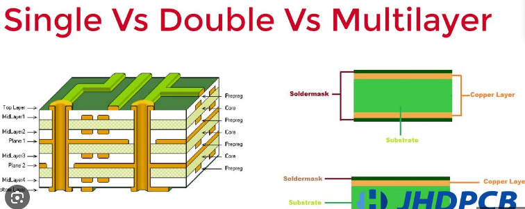
Single layer and multilayer pcb
Advantages Of Single Layer PCBs In Simple Electronic Devices
Single layer printed circuit boards (PCBs) have long been a cornerstone in the realm of electronics, particularly in the design and manufacture of simple electronic devices. These PCBs, characterized by their single conductive layer, offer a range of advantages that make them an ideal choice for straightforward applications.
One of the primary benefits of single layer PCBs is their cost-effectiveness.
The manufacturing process for these boards is relatively simple, involving fewer steps and materials compared to their multilayer counterparts. This simplicity translates to lower production costs, making single layer PCBs an economical option for mass production of basic electronic devices.
In addition to cost savings, single layer PCBs are also easier to design and manufacture.
The straightforward layout of a single conductive layer simplifies the design process, reducing the likelihood of errors and the need for complex design software. This ease of design is particularly advantageous for small-scale manufacturers and hobbyists who may not have access to advanced design tools. Furthermore, the manufacturing process for single layer PCBs is less prone to defects, as there are fewer layers to align and fewer opportunities for misalignment or other issues to occur.
Another significant advantage of single layer PCBs is their reliability.
With only one conductive layer, there are fewer points of failure, which enhances the overall durability and longevity of the device. This reliability is crucial for simple electronic devices that are expected to perform consistently over time without frequent maintenance or repairs. Additionally, the reduced complexity of single layer PCBs means that they are easier to troubleshoot and repair if issues do arise. Technicians can quickly identify and address problems, minimizing downtime and ensuring that devices remain operational.
The compact nature of single layer PCBs also contributes to their suitability for simple electronic devices.
These boards can be designed to fit into small enclosures, making them ideal for applications where space is limited. This compactness does not come at the expense of performance, as single layer PCBs can still support a wide range of electronic components and functionalities. For instance, they are commonly used in household appliances, toys, and basic consumer electronics, where their small size and reliable performance are highly valued.
Moreover, single layer PCBs are environmentally friendly. The reduced material usage and simpler manufacturing process result in less waste and lower energy consumption.
This environmental benefit is increasingly important in today’s world, where sustainability and eco-friendliness are becoming key considerations in product design and manufacturing. By choosing single layer PCBs, manufacturers can contribute to reducing the environmental impact of their products.
In conclusion, single layer PCBs offer numerous advantages for simple electronic devices, including cost-effectiveness, ease of design and manufacture, reliability, compactness, and environmental friendliness. These benefits make them an attractive option for a wide range of applications, from household appliances to basic consumer electronics. As technology continues to evolve, the enduring value of single layer PCBs in simple electronic devices remains clear, underscoring their importance in the electronics industry.
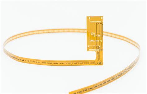
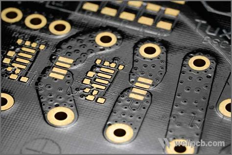
The Role Of Multilayer PCBs In Advanced Technology Applications
In the realm of modern electronics, the evolution from single-layer to multilayer printed circuit boards (PCBs) has been pivotal in advancing technology applications. Single-layer PCBs, characterized by a single conductive layer of copper, have long been the foundation of simple electronic devices. However, as the demand for more complex and compact devices has surged, the limitations of single-layer PCBs have become increasingly apparent. This has led to the widespread adoption of multilayer PCBs, which consist of multiple layers of conductive material separated by insulating layers, offering a myriad of advantages in advanced technology applications.
One of the primary benefits of multilayer PCBs is their ability to support higher component density.
In single-layer PCBs, the available surface area for placing components is limited, which restricts the complexity and functionality of the circuit. Multilayer PCBs, on the other hand, provide additional layers that can be used for routing connections, thereby freeing up surface space for more components. This increased density is crucial in applications such as smartphones, laptops, and other compact electronic devices where space is at a premium.
Moreover, multilayer PCBs enhance electrical performance by reducing the length of interconnections between components.
In single-layer PCBs, longer traces can lead to increased resistance and signal degradation, which can adversely affect the performance of high-speed circuits. By utilizing multiple layers, designers can create shorter and more direct paths for electrical signals, thereby minimizing resistance and improving signal integrity. This is particularly important in advanced technology applications such as telecommunications and data processing, where high-speed and reliable signal transmission is essential.
Another significant advantage of multilayer PCBs is their ability to provide better electromagnetic compatibility (EMC).
In single-layer PCBs, the close proximity of signal traces can lead to electromagnetic interference (EMI), which can disrupt the operation of the circuit. Multilayer PCBs allow for the separation of signal and power planes, which helps to reduce EMI and improve overall circuit performance. This is especially critical in applications such as aerospace and medical devices, where reliable and interference-free operation is paramount.
Furthermore, multilayer PCBs offer greater design flexibility, enabling the creation of more sophisticated and intricate circuits.
The additional layers provide more options for routing and placement, allowing designers to optimize the layout for performance, reliability, and manufacturability. This flexibility is essential in advanced technology applications such as automotive electronics and industrial control systems, where complex and highly reliable circuits are required.
In addition to these technical advantages, multilayer PCBs also contribute to the miniaturization of electronic devices.
As technology continues to advance, there is a growing demand for smaller and more portable devices. Multilayer PCBs enable the integration of more functionality into a smaller footprint, making it possible to create compact and lightweight devices without compromising performance. This trend is evident in the development of wearable technology, where the need for small, powerful, and energy-efficient circuits is driving innovation.
In conclusion, the transition from single-layer to multilayer PCBs has played a crucial role in the advancement of modern technology applications. The ability to support higher component density, enhance electrical performance, improve electromagnetic compatibility, and offer greater design flexibility has made multilayer PCBs indispensable in a wide range of industries. As technology continues to evolve, the importance of multilayer PCBs in enabling the development of more complex, reliable, and compact electronic devices will only continue to grow.

Cost Comparison: Single Layer Vs. Multilayer PCBs
When evaluating the cost implications of single-layer versus multilayer printed circuit boards (PCBs), it is essential to consider various factors that influence the overall expense. Single-layer PCBs, as the name suggests, consist of a single conductive layer of copper, which is laminated onto a non-conductive substrate. In contrast, multilayer PCBs comprise multiple layers of conductive material, separated by insulating layers, and are laminated together to form a single, cohesive unit. The cost comparison between these two types of PCBs is multifaceted, encompassing aspects such as material costs, manufacturing complexity, and application-specific requirements.
To begin with, single-layer PCBs are generally less expensive to produce due to their simpler design and manufacturing process.
The materials required for single-layer PCBs are relatively straightforward, involving a single layer of copper and a substrate, typically made of fiberglass-reinforced epoxy resin. This simplicity translates to lower material costs. Additionally, the manufacturing process for single-layer PCBs is less complex, requiring fewer steps and less sophisticated equipment. Consequently, the production time is shorter, and the labor costs are reduced, making single-layer PCBs a cost-effective option for many applications.
However, the cost advantages of single-layer PCBs must be weighed against their limitations.
Single-layer PCBs offer limited routing space and are generally suitable for simpler, low-density designs. As electronic devices become more complex and compact, the need for increased functionality and higher component density often necessitates the use of multilayer PCBs. Multilayer PCBs, with their multiple conductive layers, provide greater routing flexibility and can accommodate more complex circuitry within a smaller footprint. This capability is particularly valuable in advanced applications such as telecommunications, aerospace, and medical devices, where space constraints and performance requirements are critical.
While multilayer PCBs offer significant advantages in terms of design flexibility and functionality, they come with higher production costs.
The materials used in multilayer PCBs are more varied and include multiple layers of copper, insulating materials, and bonding agents. The manufacturing process is also more intricate, involving precise alignment and lamination of multiple layers, as well as additional drilling and plating steps to create interlayer connections. These complexities increase both the material and labor costs, making multilayer PCBs more expensive to produce than their single-layer counterparts.
Moreover, the cost of multilayer PCBs can be further influenced by the number of layers and the specific design requirements.
As the number of layers increases, so does the complexity of the manufacturing process, leading to higher costs. Additionally, specialized design features such as blind and buried vias, which are used to connect different layers without passing through the entire board, can add to the expense. Therefore, while multilayer PCBs offer enhanced performance and design capabilities, their higher production costs must be justified by the specific needs of the application.
In conclusion, the cost comparison between single-layer and multilayer PCBs is not straightforward and depends on various factors, including material costs, manufacturing complexity, and application-specific requirements. Single-layer PCBs are generally more cost-effective for simpler designs with lower component density, while multilayer PCBs, despite their higher production costs, provide the necessary functionality and compactness for more complex applications. Ultimately, the choice between single-layer and multilayer PCBs should be guided by a careful consideration of the specific needs and constraints of the project at hand.
Design Considerations For Single Layer And Multilayer PCBs
When designing printed circuit boards (PCBs), engineers must carefully consider whether to use single-layer or multilayer configurations. Each type has distinct advantages and limitations, and the choice between them can significantly impact the performance, cost, and manufacturability of the final product. Understanding the design considerations for both single-layer and multilayer PCBs is crucial for making an informed decision.
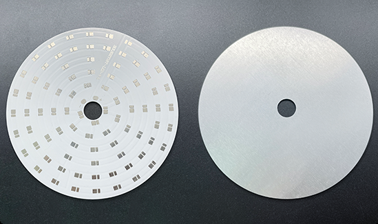
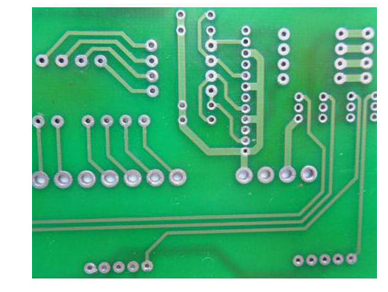
Single-layer PCBs, as the name suggests, consist of a single layer of conductive material, typically copper, on one side of a non-conductive substrate.
These boards are relatively simple and cost-effective to produce, making them ideal for low-complexity applications such as basic consumer electronics, simple sensors, and low-frequency analog circuits. The straightforward design of single-layer PCBs allows for easier troubleshooting and repair, as all components and traces are accessible from one side. However, the simplicity of single-layer PCBs also imposes limitations on their functionality. The available surface area for routing traces is restricted, which can lead to design constraints in more complex circuits. Additionally, single-layer PCBs may suffer from higher levels of electromagnetic interference (EMI) due to the lack of ground planes and shielding layers.
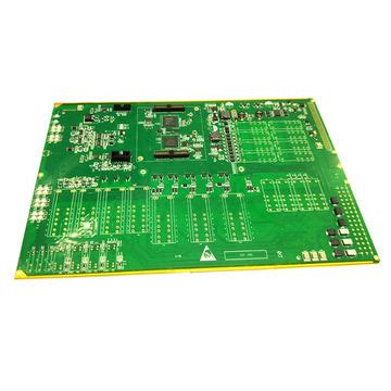
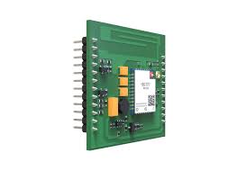
In contrast, multilayer PCBs consist of multiple layers of conductive material separated by insulating layers.
These boards can range from two layers to over a dozen, depending on the complexity of the design. Multilayer PCBs offer several advantages over their single-layer counterparts, including increased circuit density, improved signal integrity, and enhanced EMI performance. The additional layers provide more routing options, allowing for more complex and compact designs. This makes multilayer PCBs suitable for high-performance applications such as advanced computing systems, telecommunications equipment, and sophisticated medical devices.
However, the benefits of multilayer PCBs come with increased design complexity and cost.
The process of aligning and bonding multiple layers requires precise manufacturing techniques, which can drive up production costs. Additionally, the design phase for multilayer PCBs is more intricate, as engineers must carefully plan the placement of components and routing of traces across multiple layers to avoid issues such as crosstalk and signal degradation. Thermal management also becomes more challenging in multilayer designs, as the increased density of components and traces can lead to hotspots that must be mitigated through careful layout and the use of thermal vias.
When deciding between single-layer and multilayer PCBs, engineers must weigh the specific requirements of their project.
For simple, low-cost applications, single-layer PCBs may be sufficient and offer the advantage of easier manufacturing and maintenance. On the other hand, for high-performance or space-constrained applications, the benefits of multilayer PCBs often outweigh the additional complexity and cost. It is also important to consider factors such as signal integrity, EMI performance, and thermal management, as these can significantly impact the reliability and functionality of the final product.
In conclusion, the choice between single-layer and multilayer PCBs is a critical decision in the design process that requires careful consideration of various factors. By understanding the advantages and limitations of each type, engineers can make informed decisions that align with the specific needs and constraints of their projects. Whether opting for the simplicity of single-layer PCBs or the advanced capabilities of multilayer designs, the key is to balance performance, cost, and manufacturability to achieve the desired outcome.