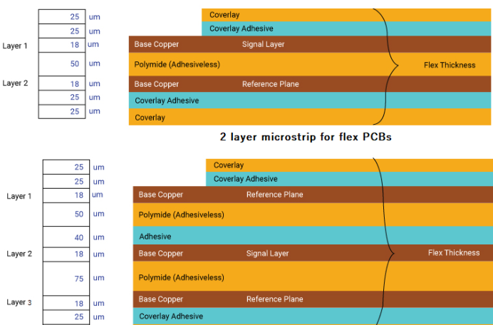
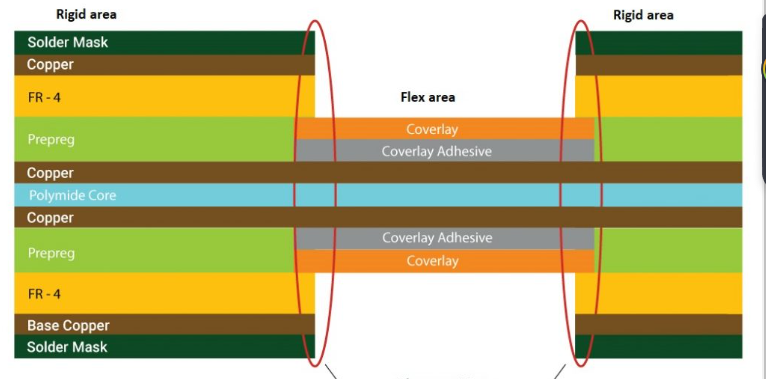
Single layer flex pcb stackup
Benefits Of Single Layer Flex PCB Stackup
Single layer flex PCB stackup offers a multitude of benefits that make it an attractive option for various electronic applications.
One of the primary advantages is its inherent flexibility, which allows for the design of circuits that can bend and twist without compromising their functionality.
This flexibility is particularly beneficial in applications where space constraints and dynamic movements are prevalent, such as in wearable technology, medical devices, and aerospace components. By enabling the creation of compact and lightweight designs, single layer flex PCBs contribute to the miniaturization of electronic devices, which is a critical factor in the advancement of modern technology.
In addition to their flexibility, single layer flex PCBs are known for their durability and reliability.
The materials used in their construction, such as polyimide or polyester films, provide excellent resistance to environmental factors like moisture, temperature variations, and chemical exposure. This robustness ensures that the circuits can withstand harsh operating conditions, thereby extending the lifespan of the devices in which they are used. Furthermore, the reduced number of layers in a single layer flex PCB minimizes the potential for interlayer delamination and other mechanical failures, enhancing the overall reliability of the circuit.
Another significant benefit of single layer flex PCB stackup is the simplification of the manufacturing process.
With only one conductive layer to work with, the design and fabrication of these PCBs are less complex compared to their multi-layer counterparts. This simplicity translates to lower production costs and shorter lead times, making single layer flex PCBs an economical choice for both prototyping and mass production. Additionally, the reduced material usage in single layer designs contributes to cost savings and aligns with sustainable manufacturing practices, which are increasingly important in today’s environmentally conscious market.
The electrical performance of single layer flex PCBs is also noteworthy.
The absence of multiple layers reduces the risk of signal interference and crosstalk, which can degrade the performance of electronic circuits. This characteristic is particularly advantageous in high-frequency applications where maintaining signal integrity is crucial. Moreover, the single conductive layer allows for straightforward routing of electrical paths, facilitating efficient signal transmission and reducing the likelihood of design errors. As a result, single layer flex PCBs are well-suited for applications that demand high precision and reliability.
Furthermore, the versatility of single layer flex PCBs extends to their compatibility with various assembly techniques.
They can be easily integrated with surface mount technology (SMT) and through-hole components, providing designers with the flexibility to choose the most appropriate assembly method for their specific application. This adaptability enhances the design freedom and allows for the creation of innovative and customized solutions that meet the unique requirements of different industries.
In conclusion, the benefits of single layer flex PCB stackup are manifold, encompassing flexibility, durability, cost-effectiveness, and superior electrical performance.
These attributes make them an ideal choice for a wide range of applications, from consumer electronics to industrial and medical devices. As technology continues to evolve, the demand for compact, reliable, and high-performance electronic solutions will only increase, further solidifying the importance of single layer flex PCBs in the future of electronic design and manufacturing.
Design Considerations For Single Layer Flex PCB Stackup
When designing a single layer flex PCB stackup, several critical considerations must be taken into account to ensure optimal performance and reliability. The unique properties of flexible PCBs, such as their ability to bend and twist, necessitate a different approach compared to rigid PCBs. One of the primary factors to consider is the choice of materials. The substrate material, typically polyimide, must be selected for its flexibility, thermal stability, and electrical insulation properties. Polyimide is favored due to its excellent mechanical and thermal characteristics, which are essential for maintaining the integrity of the circuit during flexing and thermal cycling.
In addition to the substrate, the choice of conductive material is equally important.
Copper is the most commonly used conductor due to its excellent electrical conductivity and ductility. However, the thickness of the copper layer must be carefully chosen to balance flexibility and current-carrying capacity. Thicker copper layers provide better current handling but reduce the flexibility of the PCB. Conversely, thinner copper layers enhance flexibility but may not support higher current loads. Therefore, a thorough analysis of the electrical requirements and mechanical constraints is necessary to determine the optimal copper thickness.
Another crucial aspect of single layer flex PCB stackup design is the adhesive system used to bond the copper to the substrate.
The adhesive must provide strong adhesion while maintaining flexibility and thermal stability. Acrylic and epoxy adhesives are commonly used, with each offering distinct advantages. Acrylic adhesives are known for their flexibility and resistance to thermal cycling, making them suitable for dynamic flex applications. Epoxy adhesives, on the other hand, offer superior mechanical strength and chemical resistance, which are beneficial in harsh environments.
The layout of the circuit also plays a significant role in the performance of a single layer flex PCB.
Trace routing should be designed to minimize stress concentrations and avoid sharp bends, which can lead to mechanical failure. Gentle curves and wider trace widths can help distribute stress more evenly across the flex PCB. Additionally, the use of hatched ground planes instead of solid ones can reduce the overall stiffness of the PCB, enhancing its flexibility without compromising electrical performance.
Thermal management is another important consideration in the design of single layer flex PCBs.
The flexible nature of these PCBs can lead to challenges in dissipating heat, especially in high-power applications. Incorporating thermal vias and heat spreaders can help manage heat dissipation effectively. Moreover, selecting materials with high thermal conductivity can aid in maintaining the thermal performance of the PCB.
Furthermore, the environmental conditions in which the flex PCB will operate must be considered.
Factors such as temperature extremes, humidity, and exposure to chemicals can impact the longevity and reliability of the PCB. Protective coatings, such as conformal coatings or encapsulants, can be applied to shield the PCB from environmental stressors. These coatings provide an additional layer of protection, ensuring the PCB’s performance remains consistent over its intended lifespan.
In conclusion, designing a single layer flex PCB stackup requires a comprehensive understanding of material properties, electrical and mechanical requirements, and environmental conditions. By carefully selecting materials, optimizing circuit layout, and implementing effective thermal management strategies, designers can create flexible PCBs that meet the demands of various applications. The integration of these considerations ensures that the final product not only performs reliably but also withstands the mechanical and environmental challenges it may encounter.
Common Applications Of Single Layer Flex PCB Stackup
Single layer flex PCB stackups are increasingly becoming a cornerstone in modern electronics due to their versatility and efficiency. These flexible printed circuit boards, characterized by a single conductive layer, offer a range of benefits that make them suitable for various applications. One of the most common applications of single layer flex PCB stackups is in consumer electronics. Devices such as smartphones, tablets, and wearable technology often require compact and lightweight components. The flexibility of these PCBs allows for innovative design solutions, enabling manufacturers to create thinner and more ergonomic products. Additionally, the ability to bend and fold these circuits without compromising their functionality makes them ideal for devices that demand high durability and reliability.
Another significant application of single layer flex PCB stackups is in the automotive industry.
Modern vehicles are equipped with numerous electronic systems, from advanced driver-assistance systems (ADAS) to infotainment units. The compact nature of single layer flex PCBs allows for efficient space utilization within the constrained environments of automotive interiors. Moreover, their resilience to vibrations and mechanical stress ensures long-term performance, which is crucial for automotive applications. The adaptability of these PCBs also facilitates the integration of various sensors and control units, enhancing the overall functionality and safety of vehicles.
In the medical field, single layer flex PCB stackups are indispensable in the development of medical devices. Equipment such as hearing aids, pacemakers, and diagnostic tools benefit from the lightweight and flexible properties of these PCBs. The ability to conform to different shapes and sizes allows for the creation of more comfortable and user-friendly medical devices. Furthermore, the reliability and precision of single layer flex PCBs are critical in ensuring the accuracy and effectiveness of medical treatments and diagnostics.
The aerospace industry also leverages the advantages of single layer flex PCB stackups.
In this sector, weight reduction is a paramount concern, and the lightweight nature of these PCBs contributes significantly to this goal. Their flexibility and durability make them suitable for use in various aerospace applications, including satellite systems, avionics, and communication devices. The harsh conditions of aerospace environments, such as extreme temperatures and vibrations, necessitate the use of robust and reliable components, and single layer flex PCBs meet these stringent requirements.
Moreover, industrial applications benefit from the use of single layer flex PCB stackups.
In manufacturing and automation systems, these PCBs are used in sensors, control panels, and robotic systems. Their ability to withstand harsh industrial environments, including exposure to chemicals and mechanical stress, ensures consistent performance and longevity. The flexibility of these PCBs also allows for easier installation and maintenance, reducing downtime and improving overall efficiency.
In summary, single layer flex PCB stackups are integral to a wide range of applications across various industries. Their unique properties, including flexibility, lightweight, and durability, make them suitable for consumer electronics, automotive systems, medical devices, aerospace applications, and industrial equipment. As technology continues to advance, the demand for innovative and efficient electronic components will only grow, further solidifying the importance of single layer flex PCB stackups in the modern world.
Manufacturing Process Of Single Layer Flex PCB Stackup
The manufacturing process of a single layer flex PCB stackup is a meticulous and intricate procedure that demands precision and expertise. It begins with the selection of appropriate materials, which is crucial for ensuring the flexibility and durability of the final product. Typically, a single layer flex PCB consists of a flexible substrate, such as polyimide, which is chosen for its excellent thermal stability and mechanical properties. This substrate serves as the foundation upon which the entire circuit is built.
Once the substrate is selected, the next step involves the application of a conductive layer, usually made of copper.
This copper layer is laminated onto the flexible substrate using an adhesive. The lamination process must be carefully controlled to ensure uniform adhesion and to prevent any air bubbles or imperfections that could compromise the integrity of the circuit. Following lamination, the copper layer is subjected to a photolithographic process, where a photoresist material is applied and patterned using ultraviolet light. This step is critical for defining the circuit traces and pads on the PCB.
After the photolithographic process, the exposed copper is etched away using a chemical solution, leaving behind the desired circuit pattern.
The remaining photoresist is then stripped off, revealing the copper traces that form the electrical pathways of the PCB. At this stage, the PCB undergoes a thorough inspection to ensure that the etching process has been executed correctly and that there are no defects in the circuit pattern.
Subsequently, a protective layer, often referred to as a coverlay or solder mask, is applied to the PCB.
This layer serves to insulate the copper traces and protect them from environmental factors such as moisture and contaminants. The coverlay is typically made of a flexible polymer material that is laminated onto the PCB and then cured to form a durable protective coating. Openings are created in the coverlay to expose the pads and vias, which will later be used for component mounting and electrical connections.
The next phase involves the drilling of holes, or vias, in the PCB.
These vias are essential for creating electrical connections between different layers of the PCB or for mounting components. The drilling process must be executed with high precision to ensure that the vias are accurately positioned and that their diameters are within specified tolerances. Once the vias are drilled, they are plated with copper to establish electrical continuity.
Following the drilling and plating of vias, the PCB undergoes a series of surface finishing processes.
These processes include the application of a surface finish, such as immersion gold or HASL (Hot Air Solder Leveling), to the exposed copper pads. The surface finish enhances the solderability of the pads and provides additional protection against oxidation.
Finally, the PCB is subjected to a series of electrical tests to verify its functionality and to ensure that there are no short circuits or open circuits. These tests are critical for confirming that the PCB meets the required specifications and performance standards. Once the PCB passes all tests, it is ready for component assembly and integration into electronic devices.
In conclusion, the manufacturing process of a single layer flex PCB stackup involves a series of carefully controlled steps, each of which is essential for producing a high-quality, reliable, and flexible circuit board. From material selection and lamination to photolithography, etching, drilling, and surface finishing, each stage requires precision and expertise to ensure the final product meets the stringent demands of modern electronic applications.


