Solutions to the core problems of PCB design
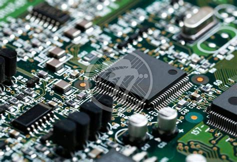
Printed circuit board (PCB) design refers to the design of schematic drawings, circuit layout, and production of circuit boards at the lowest possible cost. In the past, this usually required the help of expensive special tools, but now, with the increasing popularity of free high-performance software tools – such as DesignSpark PCB – and design models, the design speed of circuit board designers has been greatly accelerated.
Although engineering designers know that a perfect design is the best way to avoid problems, it is still a waste of time and money, and a way to treat the symptoms rather than the root cause. For example, if problems are found during the electromagnetic compatibility (EMC) testing phase, it will cause a lot of cost investment, and even the original design needs to be adjusted and remade, which will take months.
Layout is the first problem that designers face.
This problem depends on some of the contents of the drawings, and some devices need to be set together based on logical considerations. However, it should be noted that temperature-sensitive components, such as sensors, should be set separately from heat-generating components, including power converters. For designs with multiple power settings, 12V and 15V power converters can be placed in different locations on the board, because the heat and electronic noise they generate can affect the reliability and performance of other components and the board.
The above components also affect the electromagnetic performance of the circuit design,
which is not only important for the performance and energy consumption of the board, but also for the economics of the board. Therefore, all board devices sold in Europe must obtain the CE mark to prove that they will not interfere with other systems. However, this is usually only from the power supply side. There are many devices that emit noise, such as DC-DC converters and high-speed data converters. Due to defects in the board design, this noise can be captured by the channel and radiated as a small antenna, resulting in spurious noise and frequency anomalies.
The problem of far-field electromagnetic interference (EMI) can be solved by adding filters at the noise point or using metal casings to shield the signal. However, paying full attention to the devices on the board that can release electromagnetic interference (EMI) allows the board to use cheaper casings, thereby effectively reducing the cost of the entire system.
In the design process of the board, electromagnetic interference (EMI) is indeed a factor that must be taken seriously.
Electromagnetic crosstalk can couple with the channel, disrupting the signal into noise and affecting the overall performance of the board. If the coupled noise is too high, the signal may be completely overwhelmed, and more expensive signal amplifiers must be installed to restore normality. However, if the signal line layout can be fully considered at the beginning of the board design, the above problems can be avoided. Since the design of the board will vary according to different devices, different usage locations, different heat dissipation requirements, and different electromagnetic interference (EMI) conditions, design templates come in handy at this time.
Capacitance is also an important issue that cannot be ignored in board design because it affects the propagation speed of signals and increases power consumption.
Channels can couple with adjacent lines or cross two circuit layers vertically, thus inadvertently forming a capacitor. The above problems can be relatively easily solved by reducing the length of parallel lines and adding a kink to one of the lines to cut off the coupling. However, this also requires engineers to fully consider production design principles to ensure that the design is easy to manufacture and avoid any noise radiation caused by excessive line bends. Lines can also be too close together, which can create short loops between lines, especially at bends, where metal “whiskers” can form over time. Design rule checking can often indicate areas where the risk of loops is higher than normal.
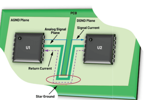
This problem is particularly prominent in the design of ground planes.
A metal circuit layer can couple with all the lines above and below it. Although this metal layer can effectively block noise, it also creates associated capacitance, which affects the speed of the line and increases power consumption.
When it comes to the design of multi-layer circuit boards, the design of through-holes between different circuit board layers is probably the most controversial issue, because through-hole design can cause many problems in the production of circuit boards. Through-holes between circuit board layers can affect the performance of signals and reduce the reliability of circuit board designs, so they should be given full attention.
Solution:
There are many different ways to solve various problems in the design process of printed circuit boards (PCBs). These include adjustments to the design itself, such as adjusting the circuit layout to reduce noise; and methods for printed circuit board layout. Design components can be automatically installed by layout tools, but if the automatic layout can be manually adjusted, it will help improve the quality of circuit board design. Through this measure, design rule detection will use technical files to ensure that the design of the circuit board meets the requirements of the circuit board manufacturer.
Separating different circuit board layers can reduce associated capacitance, but this will increase the number of layers of the circuit board, thereby increasing costs and bringing more through-hole problems. Although the use of orthogonal power supply system and ground line design may increase the physical size of the circuit board, it can effectively play the role of the ground layer in the double-layer circuit board, reducing capacitance and the complexity of circuit board manufacturing.
Design tools including DesignSpark PCB can help engineering designers solve many problems at the beginning of design, but engineering designers still need to have a full understanding of the design requirements of printed circuit boards (PCBs). For example, if the editor of the printed circuit board (PCB) needs to have some understanding of the number of layers of the circuit board at the beginning of the design, for example, a double-layer circuit board needs to have a ground layer and a power layer, two independent board layers.
Component automatic layout technology is very useful and can help designers spend more time designing the layout area of the equipment. For example, if the power supply equipment is too close to sensitive signal lines or high temperature areas, many problems will arise. Similarly, signal lines can also be automatically routed and most problems can be avoided. However, analysis and manual operation of high-risk areas will help to greatly improve the quality of printed circuit board (PCB) design, increase revenue and reduce overall costs.
Design rule detection is also a very powerful tool that can detect lines to ensure that the distance between lines is not too close, resulting in a short loop. However, the overall design still has high economic value. Design planning detection tools can also be used to detect and adjust power and ground layers to avoid large associated capacitance areas.
The above tools will also be of great help to Gerber and Excellon, helping them to print lines and circuit boards and drill through holes in order to produce the final design products. In this way, technical files are closely linked to circuit board manufacturers.
Conclusion:
There are many issues to consider in the design of printed circuit boards (PCBs), and tools such as DesignSpark PCB can effectively handle most of them. By adopting certain best practice guidelines, engineering designers can effectively reduce costs and improve the reliability of the board while meeting system specifications and deflecting system certification at a lower cost, thus avoiding more problems.