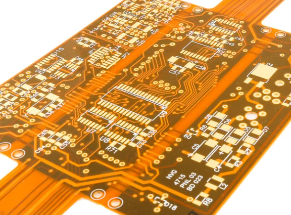
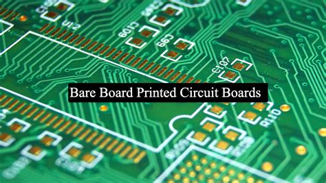
Stages of pcb manufacturing
Design And Layout
Printed Circuit Board (PCB) manufacturing is a complex process that involves several stages, each critical to the final product’s functionality and reliability. The design and layout phase is one of the most crucial steps in this process, as it sets the foundation for the entire manufacturing cycle.
This phase begins with the conceptualization of the circuit, where engineers and designers collaborate to outline the specific requirements and functionalities of the PCB. They consider factors such as the type of components to be used, the electrical connections, and the overall dimensions of the board.
Once the initial concept is clear, the next step involves creating a schematic diagram.
This diagram serves as a blueprint for the PCB, detailing the electrical connections between various components. Advanced software tools are often employed to generate these schematics, ensuring precision and accuracy. The schematic diagram is then reviewed and validated to ensure that it meets the design specifications and functional requirements. Any discrepancies or errors identified at this stage are corrected before proceeding further.
Following the schematic design, the layout process begins.
This involves placing the components on the PCB and routing the electrical connections between them. The layout must be meticulously planned to optimize space, minimize signal interference, and ensure efficient thermal management. Designers use specialized software to create a virtual model of the PCB, allowing them to experiment with different configurations and identify potential issues before physical production begins. This virtual modeling is essential for detecting and resolving problems that could compromise the board’s performance.
Transitioning from the virtual model to the physical layout, designers generate a set of Gerber files.
These files contain detailed information about each layer of the PCB, including the copper traces, solder mask, and silkscreen. Gerber files are the industry standard for PCB manufacturing and are used by fabricators to produce the physical board. The accuracy of these files is paramount, as any errors can lead to costly revisions and delays in the production process.
Once the Gerber files are finalized, they are sent to the PCB manufacturer for fabrication.
During this stage, the manufacturer uses the files to create the various layers of the PCB, starting with the copper-clad laminate. The laminate is etched to form the copper traces, which serve as the electrical pathways on the board. Subsequent layers, such as the solder mask and silkscreen, are added to protect the copper traces and provide labeling for component placement.
Throughout the design and layout phase, designers must also consider factors such as signal integrity, power distribution, and electromagnetic compatibility.
These considerations are crucial for ensuring that the PCB functions correctly in its intended application. Signal integrity involves maintaining the quality of electrical signals as they travel through the board, while power distribution ensures that all components receive the necessary voltage and current. Electromagnetic compatibility addresses the potential for electromagnetic interference, which can disrupt the operation of the PCB and other nearby electronic devices.
In conclusion, the design and layout phase of PCB manufacturing is a meticulous and iterative process that requires careful planning and attention to detail. By leveraging advanced software tools and adhering to industry standards, designers can create reliable and high-performance PCBs that meet the specific needs of their applications. This phase sets the stage for successful fabrication and assembly, ultimately leading to the production of functional and dependable electronic devices.
Material Selection
The process of printed circuit board (PCB) manufacturing is intricate and multifaceted, with each stage playing a crucial role in the final product’s performance and reliability.
One of the most critical stages in this process is material selection.
The choice of materials not only influences the electrical properties of the PCB but also affects its mechanical strength, thermal stability, and overall durability. Therefore, understanding the various materials used in PCB manufacturing and their respective properties is essential for producing high-quality circuit boards.
To begin with, the substrate material forms the foundation of the PCB.
The most commonly used substrate is FR-4, a composite material made of woven fiberglass cloth with an epoxy resin binder that is flame resistant. FR-4 is favored for its excellent balance of mechanical strength, electrical insulation, and cost-effectiveness. However, for applications requiring higher performance, such as in aerospace or high-frequency communications, alternative substrates like polyimide, PTFE (Teflon), or ceramic-based materials may be employed. These materials offer superior thermal stability and lower dielectric constants, which are crucial for maintaining signal integrity at high frequencies.
Transitioning from the substrate, the next critical material in PCB manufacturing is the copper foil.
Copper is chosen for its excellent electrical conductivity, which is essential for creating the circuit paths that connect various components on the board. The thickness of the copper foil can vary depending on the specific requirements of the PCB, with common thicknesses ranging from 1 oz/ft² to 3 oz/ft². Thicker copper layers are used in PCBs designed to handle higher currents, as they can carry more electrical load without overheating.
In addition to the substrate and copper foil, the choice of solder mask material is also pivotal.
The solder mask is a protective layer applied over the copper traces to prevent short circuits and oxidation. It also helps in the soldering process by keeping the solder confined to the designated pads. The most widely used solder mask material is epoxy liquid photoimageable (LPI) solder mask, which offers good adhesion, chemical resistance, and thermal stability. For more demanding applications, such as those involving high temperatures or harsh environments, alternative materials like polyimide or liquid crystal polymer (LCP) may be used.
Furthermore, the selection of the dielectric material between the layers of a multilayer PCB is another important consideration.
The dielectric material provides electrical insulation between the conductive layers and affects the board’s overall impedance and signal integrity. Common dielectric materials include FR-4, as well as more advanced options like Rogers materials, which offer lower dielectric constants and dissipation factors, making them suitable for high-frequency applications.
Finally, the choice of surface finish material is crucial for ensuring reliable soldering and long-term performance of the PCB.
Surface finishes protect the exposed copper pads from oxidation and provide a solderable surface. Common surface finishes include Hot Air Solder Leveling (HASL), Electroless Nickel Immersion Gold (ENIG), and Organic Solderability Preservative (OSP). Each finish has its advantages and trade-offs; for instance, HASL is cost-effective but may not be suitable for fine-pitch components, while ENIG offers excellent planarity and corrosion resistance but is more expensive.
In conclusion, material selection in PCB manufacturing is a complex and critical process that requires careful consideration of various factors, including electrical performance, mechanical strength, thermal stability, and cost. By understanding the properties and applications of different materials, manufacturers can make informed decisions that ensure the production of high-quality, reliable PCBs tailored to specific requirements.
Etching And Layering
The process of manufacturing printed circuit boards (PCBs) involves several critical stages, among which etching and layering are paramount. These stages are essential for defining the intricate pathways that allow electrical signals to travel through the board, thereby enabling the functionality of electronic devices. Understanding the nuances of etching and layering provides insight into the meticulous craftsmanship and technological precision required in PCB production.
Etching is a fundamental step in PCB manufacturing, where unwanted copper is removed from the board to create the desired circuit patterns.
Initially, a photoresist material is applied to the copper-clad laminate. This photoresist is sensitive to ultraviolet (UV) light, and when exposed through a photomask, it hardens in the areas where the circuit paths are intended to remain. The unhardened photoresist is then washed away, exposing the underlying copper.
Subsequently, the board is subjected to a chemical etching solution, typically ferric chloride or ammonium persulfate, which dissolves the exposed copper, leaving behind the precise circuit traces protected by the hardened photoresist. This process demands exact control to ensure that the etching solution removes only the unwanted copper without compromising the integrity of the circuit paths.
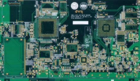
Following the etching process, the next critical stage is layering, particularly in the production of multi-layer PCBs.
Multi-layer boards are essential for complex electronic devices that require a higher density of circuits within a limited space. The layering process begins with the creation of individual etched layers, each representing a different circuit pattern. These layers are then aligned and laminated together under high pressure and temperature, using a pre-preg material, which is a fiberglass impregnated with resin. The pre-preg acts as an adhesive, bonding the layers together while providing electrical insulation between them.
To ensure the precise alignment of the layers, registration holes are drilled through the stack of layers before lamination.
These holes serve as reference points, ensuring that the circuit patterns on each layer align correctly. Once the layers are laminated, the board undergoes a curing process, solidifying the resin and creating a rigid, multi-layer structure.
After lamination, the board is drilled to create vias, which are small holes that allow electrical connections between different layers.
These vias are then plated with copper through an electroplating process, ensuring reliable electrical conductivity. The board may undergo additional etching to define the outer layer circuit patterns, followed by a solder mask application to protect the copper traces and prevent solder bridges during component assembly.
Throughout the etching and layering stages, quality control is paramount. Each step is meticulously monitored to detect any defects or misalignments that could compromise the board’s functionality. Advanced imaging and inspection technologies, such as automated optical inspection (AOI) and X-ray analysis, are employed to ensure the highest standards of precision and reliability.
In conclusion, the etching and layering stages of PCB manufacturing are intricate processes that require a high degree of precision and control. These stages are crucial for defining the circuit pathways and creating the multi-layer structures necessary for modern electronic devices. By understanding the complexities involved in etching and layering, one gains a deeper appreciation for the technological expertise and meticulous attention to detail that underpin the production of high-quality PCBs.
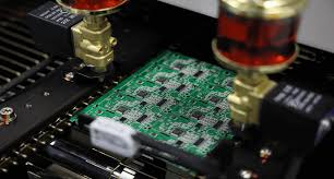
Testing And Quality Control
Testing and quality control are critical stages in the manufacturing of printed circuit boards (PCBs), ensuring that the final product meets the required standards and functions as intended. These stages involve a series of meticulous procedures designed to detect and rectify any defects or inconsistencies that may have arisen during the earlier phases of production. The importance of these processes cannot be overstated, as they directly impact the reliability and performance of the PCBs in their end-use applications.
Initially, the testing phase begins with an inspection of the raw materials used in the PCB fabrication.
This step is crucial to verify that the materials meet the specified quality standards and are free from any defects that could compromise the integrity of the final product. Following this, the PCBs undergo a series of electrical tests to ensure that the circuits are correctly formed and that there are no short circuits or open circuits. These tests are typically conducted using automated test equipment (ATE), which can quickly and accurately assess the electrical properties of the PCBs.
In addition to electrical testing, visual inspections are performed to identify any physical defects such as misaligned components, soldering issues, or surface contamination.
These inspections are often carried out using advanced imaging technologies, such as automated optical inspection (AOI) systems, which can detect even the smallest anomalies with high precision. Furthermore, X-ray inspection may be employed to examine the internal structure of the PCBs, particularly for multi-layer boards where defects may not be visible on the surface.
Another critical aspect of quality control is the functional testing of the PCBs.
This involves simulating the operating conditions under which the PCBs will be used to ensure that they perform as expected. Functional testing can include a variety of tests, such as thermal cycling, vibration testing, and humidity testing, to evaluate the PCBs’ durability and reliability under different environmental conditions. These tests help to identify any potential weaknesses that could lead to failure in the field.
Moreover, the quality control process includes a thorough review of the manufacturing documentation and process controls.
This ensures that all procedures have been followed correctly and that any deviations from the standard processes are documented and addressed. Statistical process control (SPC) techniques are often employed to monitor and control the manufacturing process, allowing for the early detection of trends that could indicate potential quality issues.
Once the PCBs have passed all the necessary tests and inspections, they are subjected to a final quality assurance review
This review involves a comprehensive evaluation of the test results and inspection reports to confirm that the PCBs meet all the specified requirements. Any PCBs that do not meet the standards are either reworked to correct the defects or discarded to prevent substandard products from reaching the customer.
In conclusion, testing and quality control are indispensable stages in PCB manufacturing, ensuring that the final products are of the highest quality and reliability. Through a combination of electrical testing, visual inspections, functional testing, and rigorous process controls, manufacturers can identify and address any defects or inconsistencies, thereby delivering PCBs that meet the stringent demands of modern electronic applications. The meticulous attention to detail in these stages underscores the commitment to excellence that is essential in the competitive field of PCB manufacturing.